All-inorganic quantum-dot light emitting diode
A quantum dot light-emitting and light-emitting diode technology, which is applied in the field of diodes, can solve the problems of high electron injection rate, quantum dot charging, and strict packaging technology requirements, so as to improve luminous efficiency, reduce absorption and blocking, and improve carrier transmission efficiency. Effect
- Summary
- Abstract
- Description
- Claims
- Application Information
AI Technical Summary
Problems solved by technology
Method used
Image
Examples
Embodiment 1
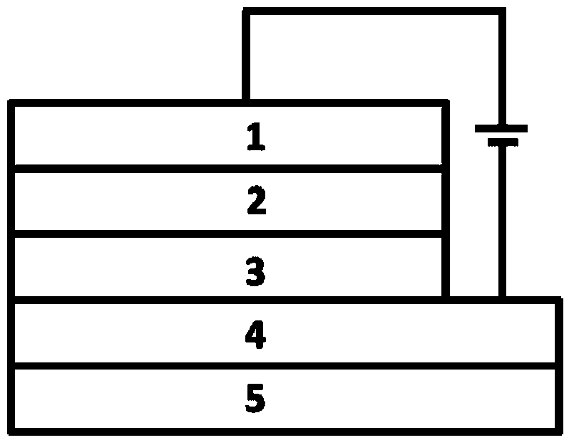
[0022] The cathode is made of commercial FTO conductive glass; the electron transport layer is TiO prepared by solvothermal method 2 Thin film with a thickness of 150nm; the light-emitting layer is CdSe with core-shell structure 2 / ZnS quantum dots, the emission peak half-maximum width is 28nm; the luminous efficiency of quantum dots is 84.6%; the anode is a metal aluminum film deposited by evaporation method, and its thickness is 80nm.
Embodiment 2
[0024] The cathode uses commercial FTO conductive glass; the electron transport layer is anatase and rutile doped structure n-type semiconductor TiO with oxygen ion vacancies prepared by solvothermal method 1.2 Thin film with a thickness of 150nm; the light-emitting layer is CdSe with a core-shell structure prepared by colloidal method 2 / ZnS quantum dots, the emission peak half-maximum width is 28nm; the luminous efficiency of quantum dots is 84.6%; the anode is a metal aluminum film deposited by evaporation method, and its thickness is 80nm.
Embodiment 3
[0026] The cathode uses commercial FTO conductive glass; the electron transport layer is anatase and rutile doped structure n-type semiconductor TiO with oxygen ion vacancies prepared by solvothermal method 1.2 Thin film with a thickness of 150nm; the light-emitting layer is Cd with core-shell structure prepared by colloidal method 1.2 Se 0.8 / ZnS quantum dots, the half-maximum width of the emission peak is 32nm; the luminous efficiency of the quantum dots is 86%; the anode is a metal aluminum film deposited by evaporation method, and its thickness is 80nm.
PUM
 Abstract
Description
Claims
Application Information
 - R&D Engineer
- R&D Manager
- IP Professional
- Industry Leading Data Capabilities
- Powerful AI technology
- Patent DNA Extraction
Browse by: Latest US Patents, China's latest patents, Technical Efficacy Thesaurus, Application Domain, Technology Topic, Popular Technical Reports.
© 2024 PatSnap. All rights reserved.Legal|Privacy policy|Modern Slavery Act Transparency Statement|Sitemap|About US| Contact US: help@patsnap.com


