Method for manufacturing quasi-monocrystalline silicon solar cells
A technology of solar cells and manufacturing methods, which is applied in the field of solar cells, can solve the problems of being lower than monocrystalline silicon cells, and that cells cannot obtain the advantages of quasi-single crystal silicon chips, and achieve uniform performance, improve photoelectric conversion efficiency, and reduce Effect of shading area
- Summary
- Abstract
- Description
- Claims
- Application Information
AI Technical Summary
Problems solved by technology
Method used
Image
Examples
Embodiment 1
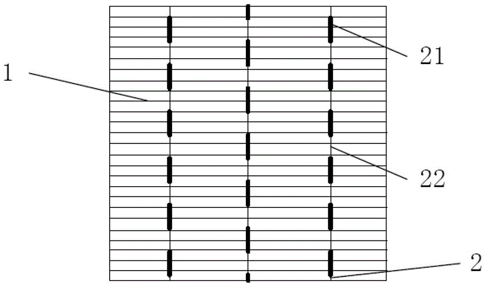
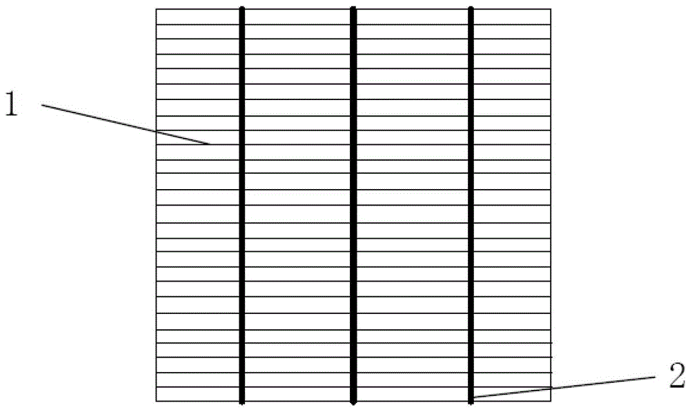
[0030] The present invention is a kind of manufacture method of quasi-single crystal silicon solar cell, it is characterized in that comprising the following steps successively:
[0031] S1. Texturing process: make a textured surface on the surface of the quasi-single crystal silicon wafer and clean it. The specific process is: first use a mixture of hydrofluoric acid and nitric acid to remove defects and mechanical damage layers on the surface of the quasi-single crystal silicon wafer. The total volume percentage of acid and nitric acid is 50~80%, the volume ratio of hydrofluoric acid and nitric acid is 1:6~7, preferably the volume ratio of hydrofluoric acid and nitric acid is 70:460, and then wash with deionized water , and then use a mixture of hydrochloric acid and nitric acid to remove the metal ion impurities on the surface of the quasi-single crystal silicon wafer, then wash it with deionized water, and finally dry the quasi-single crystal silicon wafer with compressed a...
Embodiment 2
[0042] On the basis of Example 1, this embodiment is preferred: after the quasi-single crystal silicon wafer is cleaned with a mixture of hydrofluoric acid and nitric acid in the step S1, the quasi-single crystal silicon wafer is also cleaned with lye, and then hydrochloric acid is used to clean the quasi-single crystal silicon wafer. and nitric acid to remove metal ion impurities on the surface of quasi-single crystal silicon wafers.
[0043] After the quasi-single crystal 156 silicon wafer undergoes the texturing process, the surface reflectance is tested, and the result is 21%; after the S2 light doping diffusion treatment, the square resistance value is tested, and the result is above 75Ω / □. The photoelectric conversion efficiency of the cell was tested under the conditions of AM1.5, temperature 25°C, and light intensity 1000W, and the result was 17.85~17.90%.
PUM
| Property | Measurement | Unit |
|---|---|---|
| reflectance | aaaaa | aaaaa |
| reflectance | aaaaa | aaaaa |
| reflectance | aaaaa | aaaaa |
Abstract
Description
Claims
Application Information
 - R&D
- Intellectual Property
- Life Sciences
- Materials
- Tech Scout
- Unparalleled Data Quality
- Higher Quality Content
- 60% Fewer Hallucinations
Browse by: Latest US Patents, China's latest patents, Technical Efficacy Thesaurus, Application Domain, Technology Topic, Popular Technical Reports.
© 2025 PatSnap. All rights reserved.Legal|Privacy policy|Modern Slavery Act Transparency Statement|Sitemap|About US| Contact US: help@patsnap.com


