Pixel driving circuit and method for organic light emitting diode
一种像素驱动电路、发光二极管的技术,应用在仪器、静态指示器等方向,能够解决有机发光二极管发光不稳定、增大、发光不均匀等问题,达到方便缺陷分析的效果
- Summary
- Abstract
- Description
- Claims
- Application Information
AI Technical Summary
Problems solved by technology
Method used
Image
Examples
Embodiment Construction
[0032] In order to further illustrate the technical means adopted by the present invention and its effects, the following describes in detail in conjunction with preferred embodiments of the present invention and accompanying drawings.
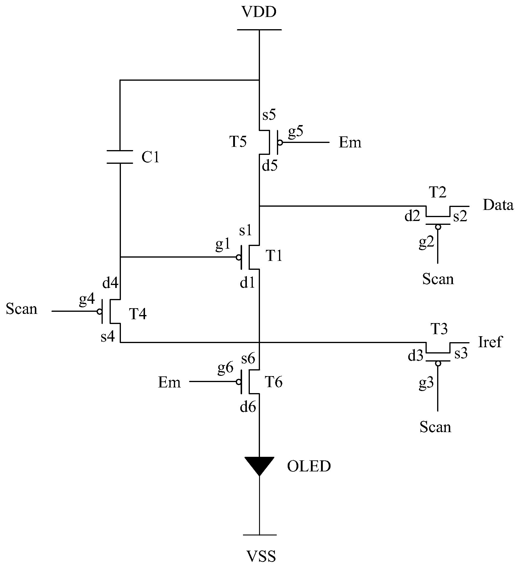
[0033] see image 3 , is the structural diagram of the 6T1C compensation circuit used in the present invention, taking the internal compensation circuit for a single pixel as an example. Including: first transistor (T1), second transistor (T2), third transistor (T3), fourth transistor (T4), fifth transistor (T5), sixth transistor (T6), storage capacitor (C1), Organic light-emitting diode (OLED); also includes scanning control terminal (Scan), data signal terminal (Data), constant current source (Iref), control light-emitting signal terminal (Em), power supply voltage (VDD), and power supply negative pole (VSS) The first transistor (T1) is a drive transistor, the first transistor (T1) includes a first gate (g1), a first source (s1), and a firs...
PUM
 Abstract
Description
Claims
Application Information
 - Generate Ideas
- Intellectual Property
- Life Sciences
- Materials
- Tech Scout
- Unparalleled Data Quality
- Higher Quality Content
- 60% Fewer Hallucinations
Browse by: Latest US Patents, China's latest patents, Technical Efficacy Thesaurus, Application Domain, Technology Topic, Popular Technical Reports.
© 2025 PatSnap. All rights reserved.Legal|Privacy policy|Modern Slavery Act Transparency Statement|Sitemap|About US| Contact US: help@patsnap.com


