Ultralow ohmic contact resistance graphene transistor and preparation method thereof
An ohmic contact and graphene technology, applied in transistors, semiconductor/solid-state device manufacturing, circuits, etc., can solve problems such as limiting the development of GFETs, and achieve the effect of reducing contact resistance and increasing the maximum oscillation frequency
- Summary
- Abstract
- Description
- Claims
- Application Information
AI Technical Summary
Problems solved by technology
Method used
Image
Examples
Embodiment 1
[0040] The ultra-low-ohm contact resistance graphene transistor comprises a substrate 1 and a source 5 and a drain 7 located on the substrate 1, and is characterized in that: a channel region is formed between the source 5 and the drain 7, and the channel region From bottom to top are: graphene layer 2 , dielectric layer 3 and gate 6 .
[0041] The preferred technical solution is that the substrate 1 is SiC, Si, SiO 2 , glass or flexible insulating substrates. The flexible insulating substrate is preferably polyethylene terephthalate, polyimide or polydimethylsiloxane substrate.
[0042] A further preferred technical solution is that the material of the dielectric layer 3 is HfO 2 , ZrO 2 , La 2 o 3 、Al 2 o 3 , TlO 2 , SrTiO 3 , LaAlO 3 , Y 2 o 3 , HfO x N y , ZrO x N y , La 2 o x N y 、Al 2 o x Ny 、TiO x N y , SrTiO x N y , LaAlO x N y , Y 2 o x N y , one or more mixtures of silicates, where x=0.5-3, Y=0-2; the source (5), drain (7) and gate (6) a...
Embodiment 2
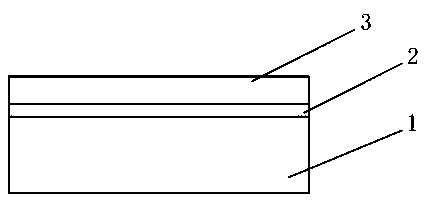
[0045] 1. A graphene layer 2 is formed on the substrate 1. The substrate of this embodiment is made of SiC material, such as figure 2 shown;
[0046] ② Deposit 4 nm Al on the graphene layer 2, and self-oxidize to form Al 2 o 3 , as dielectric layer 3, such as image 3 shown;
[0047] ③ On the dielectric layer 3, the channel area is covered by the photoresist pattern 4, such as Figure 4 shown;
[0048] ④Using the photoresist pattern 4 as a mask, the BOE solution wet etching removes the exposed dielectric layer 3 outside the channel area, such as Figure 5 shown;
[0049] 5. Use the photoresist pattern 4 as a mask, oxygen plasma etching the exposed graphene layer 2 outside the channel region, as Figure 6 shown;
[0050] ⑥Electron beam evaporation of 100 nm Au as source and drain ohmic contact metal to form ohmic contact metal layer 8, peel off, and remove photoresist pattern 4, such as Figure 7 , 8 shown;
[0051] ⑦ Cover the required source and drain regions thro...
Embodiment 3
[0055] ① Form a graphene layer 2 on the substrate 1, the substrate of this embodiment is SiO 2 Material; the graphene layer adopts the single-layer graphene prepared by tearing method, such as figure 2 shown;
[0056] ② Deposit 2 nm Ti on the graphene layer 2, and auto-oxidize to form TiO 2 , as a seed layer, on which HfO was deposited using ALD (atomic layer deposition) 2 , forming a dielectric layer 3, such as image 3 shown;
[0057] ③ On the dielectric layer 3, the channel area is covered by the photoresist pattern 4, such as Figure 4 shown;
[0058] ④ Use photoresist pattern 4 as a mask, use HNO 3 with H 2 o 2 The mixed solution wet etching removes the exposed dielectric layer 3 outside the channel area, such as Figure 5 shown;
[0059] 5. Use the photoresist pattern 4 as a mask, oxygen plasma etching the exposed graphene layer 2 outside the channel region, as Figure 6 shown;
[0060] ⑥Electron beam evaporation of 50 nm Pd as source and drain ohmic contact...
PUM
 Abstract
Description
Claims
Application Information
 - R&D
- Intellectual Property
- Life Sciences
- Materials
- Tech Scout
- Unparalleled Data Quality
- Higher Quality Content
- 60% Fewer Hallucinations
Browse by: Latest US Patents, China's latest patents, Technical Efficacy Thesaurus, Application Domain, Technology Topic, Popular Technical Reports.
© 2025 PatSnap. All rights reserved.Legal|Privacy policy|Modern Slavery Act Transparency Statement|Sitemap|About US| Contact US: help@patsnap.com


