
A kind of preparation method of anti-radiation reinforced bipolar transistor

A bipolar transistor, anti-radiation reinforcement technology, applied in the field of electronics, can solve the problem of low anti-irradiation ability of bipolar transistors, and achieve improved anti-irradiation ability, simple manufacturing process steps, and anti-irradiation ability. The effect of increasing the failure threshold

Active Publication Date: 2016-09-14
石家庄天林石无二电子有限公司 +2
View PDF4 Cites 0 Cited by
  • Summary
  • Abstract
  • Description
  • Claims
  • Application Information

AI Technical Summary

Problems solved by technology

[0004] The present invention aims to solve the problem of low radiation resistance of existing bipolar transistors, and now provides a preparation method of radiation-resistant reinforced bipolar transistors

Method used


Image

  • A kind of preparation method of anti-radiation reinforced bipolar transistor
  • A kind of preparation method of anti-radiation reinforced bipolar transistor
  • A kind of preparation method of anti-radiation reinforced bipolar transistor

Examples


specific Embodiment approach 1

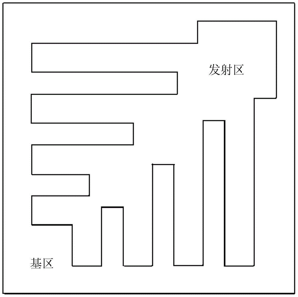
[0028] Specific implementation mode one: refer to figure 1 This implementation mode is described in detail. In the radiation-resistant reinforced bipolar transistor described in this implementation mode, the emitter region of the transistor takes the diagonal line of the base region as the symmetrical line to form a left-right symmetrical square symmetrical comb structure. N pairs of rectangular tooth structures are symmetrically extended outward on both sides of the line, the angle between each pair of rectangular tooth structures is 90 degrees, and n is a positive integer greater than 3.

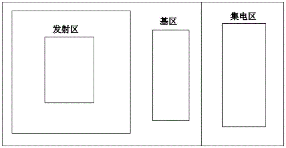
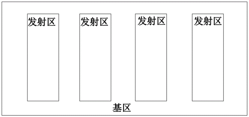
[0029] A schematic diagram of a simplified structure of a conventional bipolar transistor, such as figure 2 As shown; usually, the emitter region of the bipolar transistor adopts a rectangular comb structure, such as image 3 shown. Figure 4 After irradiation with low-energy electrons, the variation of the reciprocal current gain of bipolar transistors with different emitter perimeter / ...

specific Embodiment approach 2

[0034] Embodiment 2: This embodiment is a further description of the radiation-resistant hardened bipolar transistor described in Embodiment 1. In this embodiment, the value range of n is greater than 3 and less than 10.

specific Embodiment approach 3

[0035] Embodiment 3: This embodiment is a further description of the radiation-resistant hardened bipolar transistor described in Embodiment 1. In this embodiment, all rectangular tooth structures have the same width.


PUM


Abstract

The invention discloses a reinforced bipolar transistor resistant to radiation and a method for preparing the reinforced bipolar transistor resistant to radiation and belongs to the field of electronic techniques. The reinforced bipolar transistor resistant to radiation and the method for preparing the reinforced bipolar transistor resistant to radiation solve the problem that an existing bipolar transistor is poor in radiation resistance. According to the reinforced bipolar transistor resistant to radiation, an emitter region is of an eudipleural square comb structure with the diagonal line of a base region as the symmetric line, n pairs of rectangular tooth structures symmetrically extend outwards from the two sides of the symmetric line, and the included angle between every pair of rectangular tooth structures is 90 degrees. The method for preparing the reinforced bipolar transistor resistant to radiation comprises the steps that when doping elements diffuse to form the base region, and the diffusion junction depth of the base region is between 1 micron and 2.5 microns; a layer of boron is diffused on the surface of the base region; when the doping elements diffuse to form the emitter region, the diffusion junction depth of the emitter region is between 0.5 micron and 2 microns; during oxidation, it is guaranteed that the thickness of dry oxygen is between 1 nm and 10 nm and the thickness of wet oxygen is between 200 nm and 1 micron. The reinforced bipolar transistor resistant to radiation and the method for preparing the reinforced bipolar transistor resistant to radiation are suitable for application and production of commercial bipolar transistors resistant to radiation.

Description

technical field [0001] The invention belongs to the field of electronic technology, in particular to an anti-radiation reinforced bipolar transistor. Background technique [0002] Electrons and protons in the space radiation environment have a strong impact on the performance of electronic devices used in spacecraft, which will cause ionizing radiation effects, displacement radiation effects and single event effects, etc., leading to abnormalities or failures of electronic devices, and eventually lead to disasters in spacecraft sex accident. Therefore, improving the anti-irradiation ability of bipolar devices has very important engineering practical significance for optimizing the material selection and design of spacecraft and improving the reliability of spacecraft in orbit. [0003] The emitter perimeter / area ratio of a bipolar device is an important factor affecting its radiation resistance. After the irradiation experiment, the base current I of the bipolar device B ...

Claims


Application Information

Patent Timeline
Patent Type & Authority Patents(China)
IPC IPC(8): H01L29/73H01L29/08H01L21/331
CPCH01L29/0804H01L29/66234H01L29/73
Inventor 刘广桥李兴冀赵玉玲刘艳秋段庆禄杨剑群孙毅刘超铭李鹏伟宋桂芬何世禹
Owner 石家庄天林石无二电子有限公司
Learn More