GaN base LED transparent electrode graphical preparation method
A transparent electrode and patterning technology, applied in circuits, electrical components, semiconductor devices, etc., can solve problems such as unstable corrosion process, difficulty and danger of production personnel, complex mask process, etc., to reduce the cost and time-consuming of lithography , Reduce the harm to the human body, and improve the efficiency of light extraction
- Summary
- Abstract
- Description
- Claims
- Application Information
AI Technical Summary
Problems solved by technology
Method used
Image
Examples
Embodiment 1
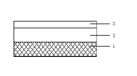
[0032] Referring to the accompanying drawings, the method for preparing a patterned transparent electrode of a GaN-based LED in this embodiment, the steps include:
[0033] 1. Evaporate ITO transparent electrodes on the GaN-based epitaxial layer by electron beam evaporation: the power of the electron beam bombardment source is 1KW, the substrate temperature is 300°C, and the vacuum degree is 2×10 -5 Torr; the thickness of the evaporated transparent electrode is 1000 ?.
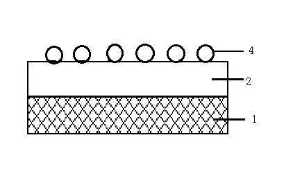
[0034] 2. Deposit a layer of ultrathin SiO on the transparent electrode by PECVD 2 Layer: growth temperature 200°C, deposited SiO 2 The thickness is 10 ?, so that during annealing, SiO 2 The chemical bonds between the molecules are broken to form a crystal pattern.
[0035] 3. Thin SiO 2 Layered GaN-based epitaxial wafers were placed in an annealing furnace at 250 °C under a nitrogen atmosphere for 5 minutes, and the SiO 2 A rhomboid β-phospho-quartz crystal pattern is generated.
[0036] 4. Use the diam...
Embodiment 2
[0040] 1. Evaporate ITO transparent electrodes on the GaN-based epitaxial layer by electron beam evaporation: the power of the electron beam bombardment source is 1KW, the substrate temperature is 300°C, and the vacuum degree is 2×10 -5 Torr; the thickness of the evaporated transparent electrode is 1000 ?.
[0041] 2. Deposit a layer of ultrathin SiO on the transparent electrode by PECVD 2 Layer: growth temperature 200°C, deposited SiO 2 The thickness is 50 ?, so that during annealing, SiO 2 The chemical bonds between the molecules are broken to form a crystal pattern.
[0042] 3. Thin SiO 2 Layered GaN-based epitaxial wafers were placed in an annealing furnace at 300 °C under a nitrogen atmosphere for 6 minutes, and the SiO 2 A trapezoidal γ-phospho-quartz crystal pattern is generated.
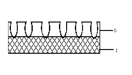
[0043] 4. Use the trapezoidal γ-phosphorous quartz crystal as the mask of the transparent electrode, and use ICP to etch the exposed transparent electrode; 2 and BCl 3 is the main gas ...
Embodiment 3
[0047] 1. Evaporate ZnO transparent electrodes on the GaN-based epitaxial layer by electron beam evaporation: the power of the electron beam bombardment source is 1KW, the substrate temperature is 300°C, and the vacuum degree is 2×10 -5 Torr; the thickness of the evaporated transparent electrode is 1500 ?.
[0048] 2. Deposit a layer of ultrathin SiO on the transparent electrode by PECVD 2 Layer: growth temperature 200°C, deposited SiO 2 The thickness is 100 ?, so that during annealing, SiO 2 The chemical bonds between the molecules are broken to form a crystal pattern.
[0049] 3. Thin SiO 2Layered GaN-based epitaxial wafers were placed in an annealing furnace at 300 °C under a nitrogen atmosphere for 7 minutes, and the SiO 2 A rhombohedral γ-phospho-quartz crystallographic pattern is generated.
[0050] 4. Use rhombic γ-phosphorous quartz crystal as the mask of the transparent electrode, and use ICP to etch the exposed transparent electrode; 2 and BCl 3 is the main ga...
PUM
 Abstract
Description
Claims
Application Information
 - R&D
- Intellectual Property
- Life Sciences
- Materials
- Tech Scout
- Unparalleled Data Quality
- Higher Quality Content
- 60% Fewer Hallucinations
Browse by: Latest US Patents, China's latest patents, Technical Efficacy Thesaurus, Application Domain, Technology Topic, Popular Technical Reports.
© 2025 PatSnap. All rights reserved.Legal|Privacy policy|Modern Slavery Act Transparency Statement|Sitemap|About US| Contact US: help@patsnap.com


