Bias voltage temperature instability testing circuit and testing method thereof

A technology for testing circuits and instability, applied in the field of integrated circuit reliability testing, can solve the problem of inability to distinguish the degree of the influence of the PMOS tube negative bias temperature unstable oscillation frequency, etc., to improve reliability and increase sensitivity. Effect

Inactive Publication Date: 2014-02-12
SEMICON MFG INT (SHANGHAI) CORP
View PDF8 Cites 6 Cited by
  • Summary
  • Abstract
  • Description
  • Claims
  • Application Information

AI Technical Summary

Problems solved by technology

[0003] figure 1 It is a schematic diagram of a bias temperature instability test circuit in the prior art. The bias temperature instability test circuit is based on a ring oscillator circuit, and the ring oscillator circuit oscillates by testing the PMOS transistor and the NMOS transistor before and after the pressure voltage is applied. Frequency conversion, testing the negative bias temperature instability of the PMOS tube and the positive bias temperature instability of the NMOS tube, but the bias temperature instability test circuit cannot distinguish between the negative bias temperature instability of the PMOS tube and the positive bias temperature instability of the NMOS tube. The degree of influence of the positive bias temperature instability of the NMOS tube on the circuit oscillation frequency

Method used


Image

  • Bias voltage temperature instability testing circuit and testing method thereof
  • Bias voltage temperature instability testing circuit and testing method thereof
  • Bias voltage temperature instability testing circuit and testing method thereof

Examples


no. 1 example

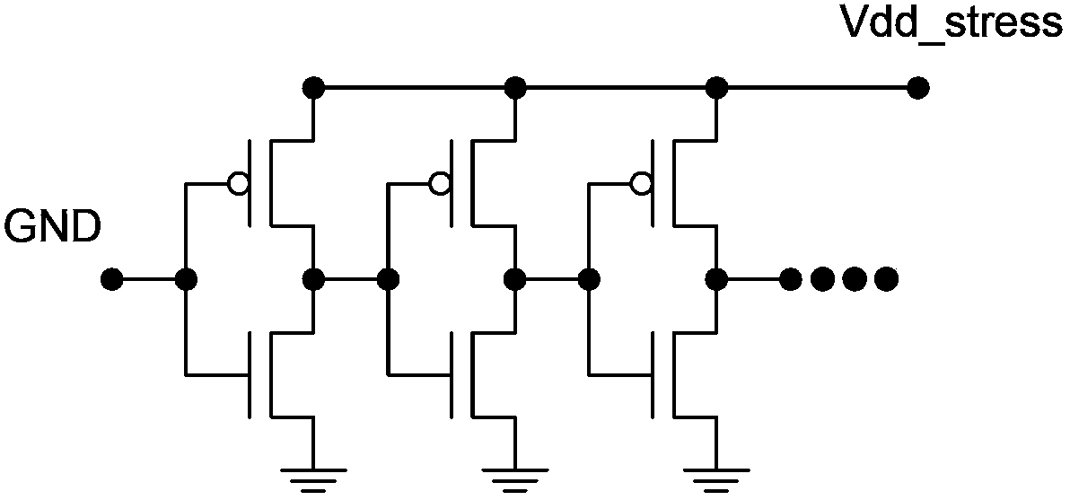
[0061] Please refer to the following figure 2 , which is a schematic diagram of the bias temperature instability test circuit according to the first embodiment of the invention.

[0062] The bias temperature instability test circuit of the present invention includes a ring resonator circuit and n-level test circuits, and each level of test circuits includes a pair of complementary PMOS transistors to be tested and NMOS transistors to be tested, a pair of complementary switch PMOS transistors and A switch NMOS transistor and a pair of complementary voltage-dividing PMOS transistors and voltage-dividing NMOS transistors.

[0063] like figure 2 As shown, in this embodiment, the bias temperature instability test circuit is based on a ring resonator circuit, and the ring oscillator circuit includes n-level test circuits, each of which has the same structure, where n is positive integer, in figure 2 Among them, S1 is the first-level test circuit, S2 is the second-level test ci...

no. 2 example

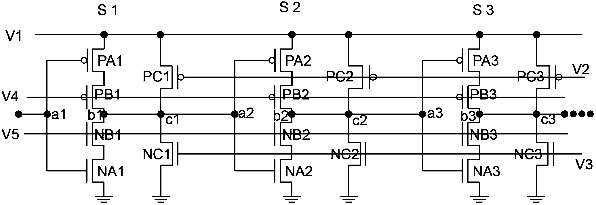
[0076] Please refer to the following Figure 5, which is a schematic diagram of a bias temperature instability test circuit according to the second embodiment of the invention. The second embodiment is based on the first embodiment, the difference is that the bias temperature instability testing circuit of the second embodiment further includes a transmission gate. A transmission gate is connected between the third node of each test circuit and the first node of the next test circuit. When k is 2, such as Figure 5 As shown, the second-level test circuit further includes a transmission gate, one end of the transmission gate is connected to the third node c2 in the second-level test circuit, and the other end of the transmission gate is connected to the first node a3 in the third-level test circuit . One end of the transmission gate in the n-level test circuit is connected to the third node cn in the n-level test circuit, and the other end is connected to the first node a1 i...


PUM


Abstract

The invention discloses a bias voltage temperature instability testing circuit which comprises a circular vibrator circuit. The vibrator circuit comprises n grades of testing circuits which are the same in structure. Each testing circuit comprises a first node, a second node and a third node. The third node of each testing circuit is connected with the first node of a former testing circuit. Each testing circuit comprises a PMOS tube to be tested, an NMOS tube to be tested, a switch PMOS tube, a switch NMOS tube and at least one pair of partial pressure PMOS tube and partial pressure NMOS tube, wherein the PMOS tube to be tested and the NMOS tube to be tested are complementary, the switch PMOS tube and the switch NMOS tube are complementary, and the partial pressure PMOS tube and the partial pressure NMOS tube are complementary. The invention further discloses a testing method for the bias voltage temperature instability testing circuit. The method comprises the steps of providing the bias voltage temperature instability testing circuit, testing the negative bias pressure temperature instability of the PMOS tube to be tested and testing the positive bias pressure temperature instability of the NMOS tube to be tested. The bias voltage temperature instability testing circuit can test the negative bias pressure temperature instability of the PMOS tube to be tested and the positive bias pressure temperature instability of the NMOS tube to be tested.

Description

technical field [0001] The invention relates to the field of integrated circuit reliability testing, in particular to a bias temperature instability testing circuit and a testing method thereof. Background technique [0002] Bias Temperature Instability (BTI for short) is one of the basic problems of reliability of Complementary Metal Oxide Semiconductor (CMOS for short). Among them, BTI is divided into negative bias temperature instability (Negative Bias Temperature Instability, referred to as NBTI) and positive bias temperature instability (Positive Bias Temperature Instability, referred to as PBTI). NBTI refers to the degradation of a series of electrical parameters caused by applying negative gate voltage to the PMOS tube at high temperature. The generation process of NBTI effect mainly involves the generation and passivation of positive charges, that is, the generation of interface trap charges and fixed positive charges in the oxide layer. As well as the diffusion pro...

Claims


Application Information

Patent Timeline
Patent Type & Authority Applications(China)
IPC IPC(8): G01R31/26
Inventor 甘正浩冯军宏
Owner SEMICON MFG INT (SHANGHAI) CORP
Why Eureka
Try Eureka