Tunneling field effect transistor of vertical structure and preparation method thereof

A technology of tunneling field effect and vertical structure, which is applied in semiconductor/solid-state device manufacturing, semiconductor devices, electrical components, etc., can solve the problems of large leakage current and small drive current of planar tunneling field effect transistors, and achieve improved drive current, suppress leakage current, and increase the effect of tunneling area

Active Publication Date: 2014-02-05
SHANGHAI INST OF MICROSYSTEM & INFORMATION TECH CHINESE ACAD OF SCI
View PDF3 Cites 3 Cited by
  • Summary
  • Abstract
  • Description
  • Claims
  • Application Information

AI Technical Summary

Problems solved by technology

[0004] In view of the above-mentioned shortcomings of the prior art, the object of the present invention is to provide a tunneling field-effect transistor with a vertical structure and its preparation method, which is used to solve the problem of small driving current and leakage of the planar tunneling field-effect transistor in the prior art. The current is still a big problem

Method used


Image

  • Tunneling field effect transistor of vertical structure and preparation method thereof
  • Tunneling field effect transistor of vertical structure and preparation method thereof
  • Tunneling field effect transistor of vertical structure and preparation method thereof

Examples


Embodiment 1

[0046] The invention provides a method for preparing a tunneling field effect transistor with a vertical structure, such as figure 1 As shown in the process flow chart, the preparation method of the tunneling field effect transistor with vertical structure at least includes the following steps:

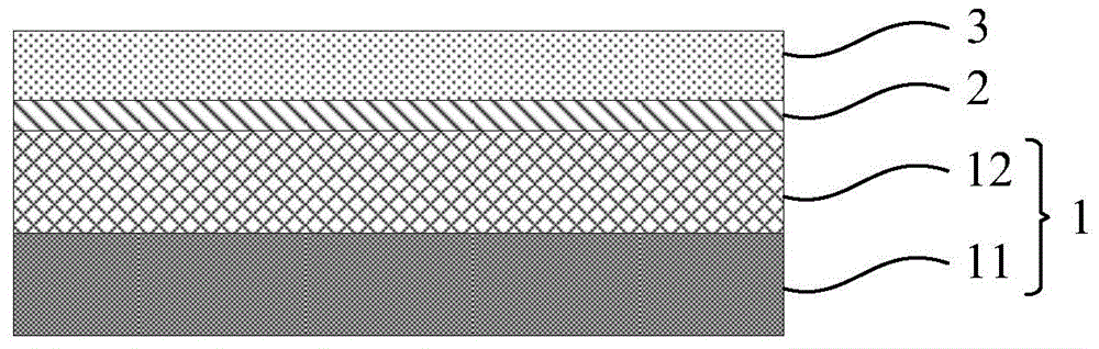
[0047] S1, providing an SGOI substrate, the SGOI substrate including a buried oxide layer and P-type heavily doped SiGe formed on the buried oxide layer;

[0048] S2, sequentially depositing a silicon layer and N-type heavily doped SiGe on the P-type heavily doped SiGe;

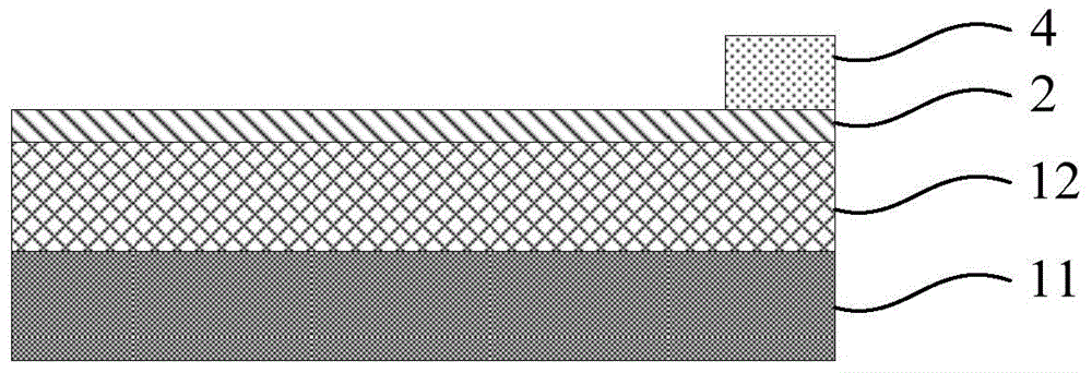
[0049] S3, using photolithography and etching techniques to etch the N-type heavily doped SiGe to form a drain on one side of the silicon layer;

[0050] S4, etching the silicon layer to form a channel with a nanowire or nanorod structure;

[0051]S5, using a chemical etching process to remove part of the P-type heavily doped SiGe under the channel, so that the channel is suspended, and the P-type heavily doped SiG...

Embodiment 2

[0076] The present invention also provides a tunneling field effect transistor with a vertical structure, which is made by using the preparation method provided in Embodiment 1. The tunneling field effect transistor with a vertical structure at least includes:

[0077] The SGOI substrate 1 includes a buried oxide layer 11 and P-type heavily doped SiGe12 located on both sides of the buried oxide layer 11, wherein the P-type heavily doped SiGe12 on one side is defined as a source 121;

[0078] A channel 21 with a nanowire or nanorod structure suspended over the P-type heavily doped SiGe12;

[0079] The drain 4 is combined with the P-type heavily doped SiGe12 on the other side opposite to the source 121, and the source 121, the channel 21 and the drain 4 form a vertical structure;

[0080] a gate dielectric layer 5 wrapped on the surface of the channel 21;

[0081] The gate 6 is formed on the gate dielectric layer 5 .

[0082] The width of the channel 21 of the nanowire or nano...


PUM

PropertyMeasurementUnit
Thicknessaaaaaaaaaa
Thicknessaaaaaaaaaa
Thicknessaaaaaaaaaa

Abstract

The invention provides a tunneling field effect transistor of a vertical structure and a preparation method thereof. The preparation method at least comprises the steps of providing an SGOI substrate which comprises an oxygen buried layer and P-type heavy dopping SiGe; sequentially sedimenting to form a silicon layer and N-type heavy dopping SiGe on the P-type heavy dopping SiGe; utilizing the photoetching and etching technology to etch the N-type heavy dopping SiGe so as to form a drain electrode on one side surface of the silicon layer; etching the silicon layer to form a ditch of a nanometer line structure or a nanometer bar structure; utilizing the chemical erosion technology to remove a part of P-type heavy dopping SiGe under the ditch so as to enable the ditch to be hung in the air, defining the P-type heave dopping SiGe on the other side opposite to the drain electrode to be a source electrode. The drain electrode, the ditch and the source electrode form a vertical structure. According to the tunneling field effect transistor of the vertical structure, the drain electrode, the ditch and the source electrode form the vertical structure, so that a tunneling area can be increased, and drive currents of elements can be improved. Further, the formed ditch hung in the air can further restrict leaked currents of elements.

Description

technical field [0001] The invention relates to the technical field of semiconductor devices, in particular to a tunneling field effect transistor with a vertical structure and a preparation method thereof. Background technique [0002] In recent years, microelectronics technology with silicon integrated circuits as the core has developed rapidly. The development of integrated circuit chips basically follows Moore's law, that is, the integration level of semiconductor chips doubles every 18 months. Over the past period of time, the advancement of microelectronics technology has been based on the continuous optimization of the cost-effectiveness of materials, processes and processes. However, scaling down conventional silicon-based CMOS transistors has become increasingly difficult with the development of microelectronics technology. Moreover, most electronic products manufactured using MOSFETs today have the following main problems: First, due to the shortening of the MOSFE...

Claims


Application Information

Patent Timeline
IPC IPC(8): H01L29/78H01L29/06H01L21/336
CPCH01L29/0603H01L29/41766H01L29/66666H01L29/7827
Inventor 赵清太俞文杰刘畅王曦
Owner SHANGHAI INST OF MICROSYSTEM & INFORMATION TECH CHINESE ACAD OF SCI
Why Eureka
Try Eureka