Insulated gate bipolar semiconductor device
A technology of N-type semiconductors and semiconductors, which is applied in the direction of semiconductor devices, semiconductor/solid-state device manufacturing, electrical components, etc., can solve the problems of increasing IGBT conduction voltage drop, high conduction voltage drop, and low hole concentration, and achieves The effect of flexible control and low conduction voltage drop
- Summary
- Abstract
- Description
- Claims
- Application Information
AI Technical Summary
Problems solved by technology
Method used
Image
Examples
Embodiment 1
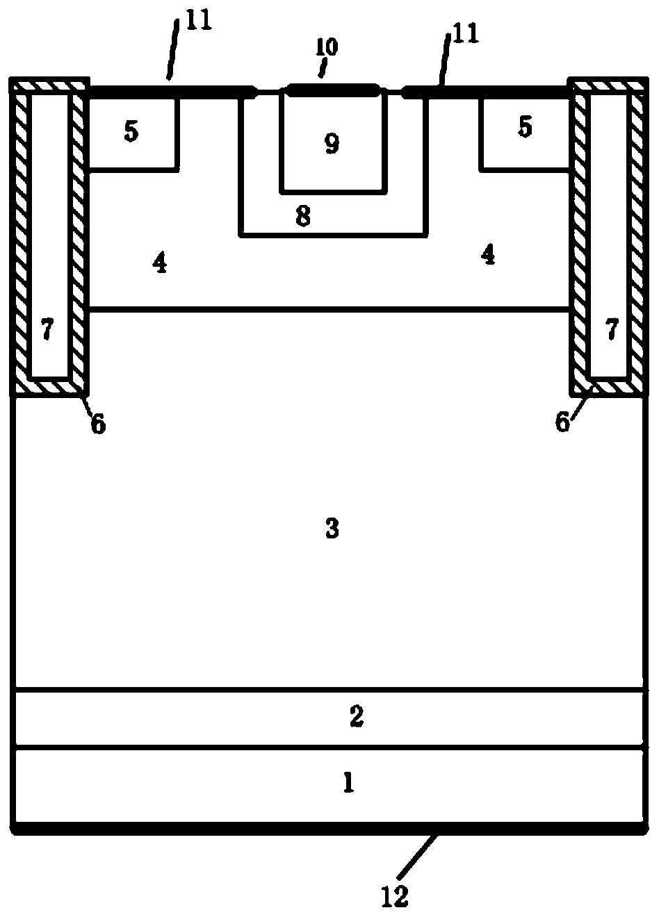
[0016] Such as figure 1 As shown, this example is an insulated gate bipolar semiconductor device with a trench gate structure, which includes a collector metal 12, a P-type semiconductor material 1, an N-type semiconductor material 2, an N-type drift region 3, and a first P-type semiconductor stacked in sequence. Body region 4 and emitter metal 11, the first P-type semiconductor body region 4 includes two mutually independent emitter regions 5; it is characterized in that it also includes a second P-type semiconductor region 8, an N-type semiconductor region 9, Oxide layer 6 and polysilicon 7; the oxide layer 6 covers the outer surface of polysilicon 7 to form two slot gate structures respectively, and the two slot gate structures are arranged at both ends of the insulated gate bipolar semiconductor device, and the slots The gate structure is respectively connected to the side of the emitter region 5 and the side of the first P-type semiconductor body region 4 and embedded in ...
Embodiment 2
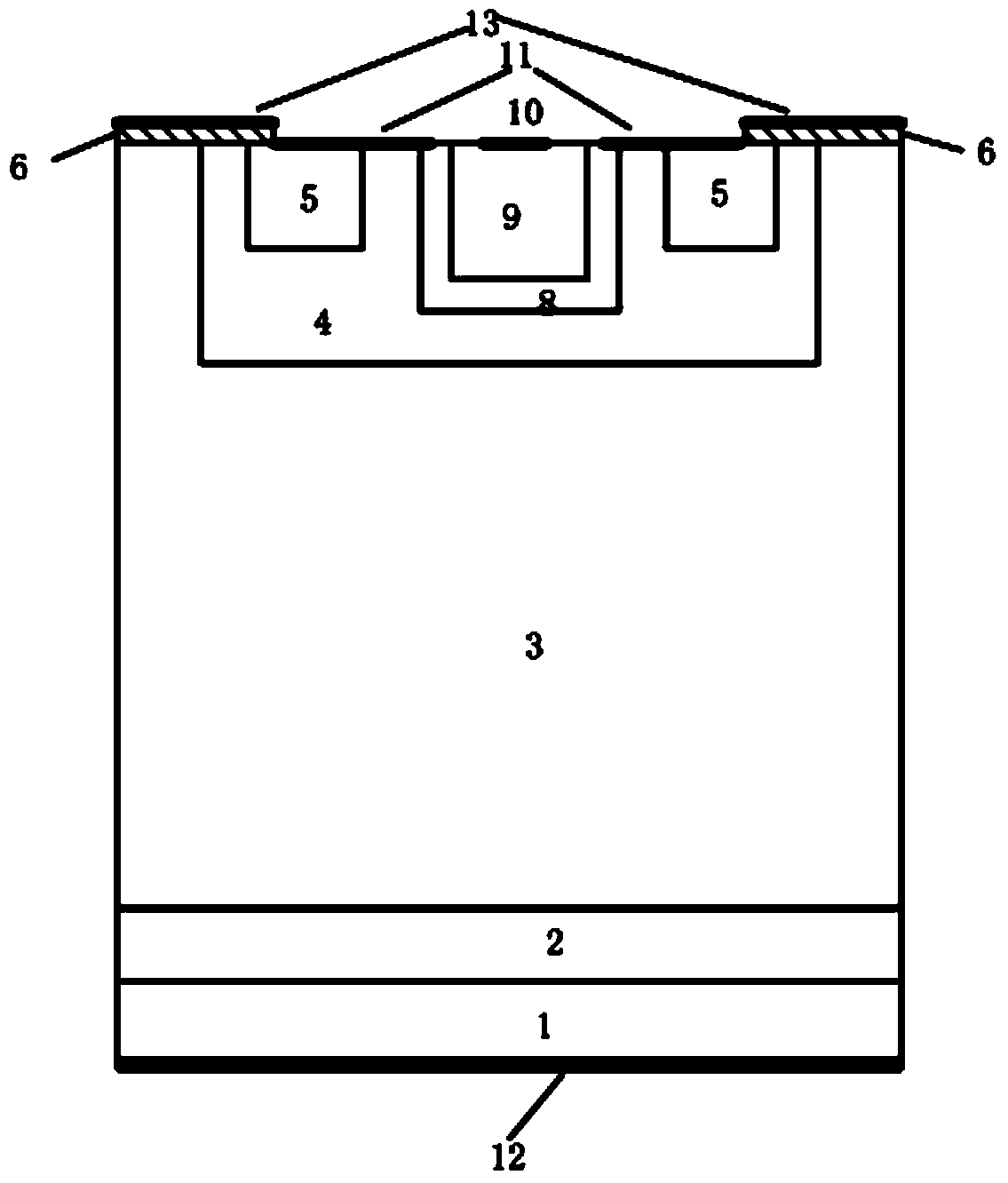
[0021] Such as figure 2 As shown, this example is an insulated gate bipolar semiconductor device with a planar gate structure. Compared with Example 1, this example has no groove gate, and the oxide layer 6 is arranged on the upper surface of the N-type drift region 3 and part of the first P-type semiconductor device. The upper surface of the body region 4 is provided with a planar gate electrode 13 on the upper surface of the oxide layer 6 .
[0022] The manufacturing method of this example is:
[0023]First perform N-type ion implantation on the back of the N-type semiconductor single crystal 3 to form a field stop layer 2, then perform boron ion implantation on the front of the N-type semiconductor single crystal 3 to form a P-type body region 4, and then perform a boron ion implantation in the body region to form a second P-type semiconductor region 8, and N-type ion implantation is performed in this region to form N-type semiconductor region 9, and then an oxide layer 6...
PUM
 Abstract
Description
Claims
Application Information
 - R&D Engineer
- R&D Manager
- IP Professional
- Industry Leading Data Capabilities
- Powerful AI technology
- Patent DNA Extraction
Browse by: Latest US Patents, China's latest patents, Technical Efficacy Thesaurus, Application Domain, Technology Topic, Popular Technical Reports.
© 2024 PatSnap. All rights reserved.Legal|Privacy policy|Modern Slavery Act Transparency Statement|Sitemap|About US| Contact US: help@patsnap.com


