LED epitaxial wafer, method for making the same, and LED chip including the same
A technology of LED epitaxial wafers and LED chips, which is applied in the direction of electrical components, circuits, semiconductor devices, etc., can solve the problems of many lattice defects and poor crystal quality of the active layer, so as to improve the luminous efficiency, improve the crystal quality, and improve the interface state and roughness effects
- Summary
- Abstract
- Description
- Claims
- Application Information
AI Technical Summary
Problems solved by technology
Method used
Image
Examples
Embodiment 1
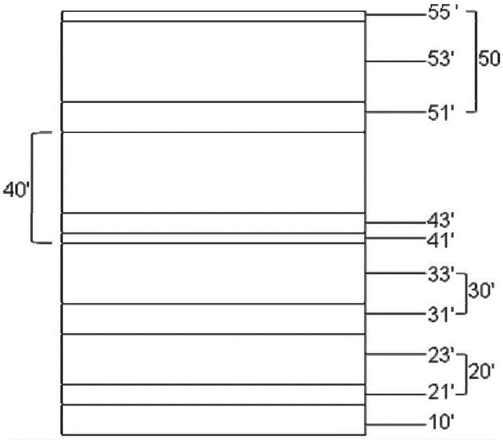
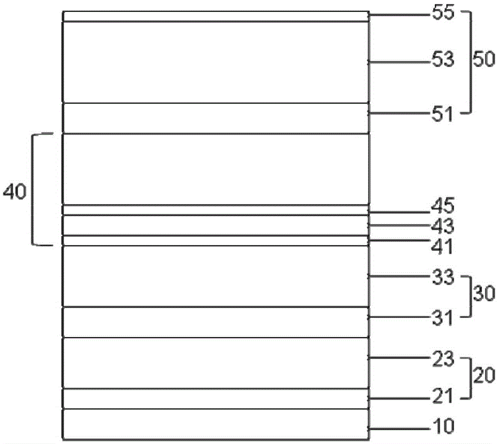
[0055] This embodiment provides a method for manufacturing an LED epitaxial wafer, comprising the following steps:
[0056] First, a GaN buffer layer, GaN layer, N-type AlGaN, and Si-doped N-type GaN are sequentially formed from the surface of the substrate outward, including the following steps:
[0057] Raise the temperature from room temperature to 1100°C, and process the substrate for 10 minutes under a hydrogen atmosphere with a pressure of 500mbar in the reaction chamber;
[0058] The temperature was lowered to 580°C, and the substrate was nitrided in a mixed atmosphere of hydrogen and nitrogen at a pressure of 500 torr in the reaction chamber. The treatment time was 5 minutes, and the volume fraction of hydrogen in the mixed atmosphere was 10%; Ethylgallium or trimethylgallium, a GaN buffer layer with a thickness of 540nm is grown on the substrate;
[0059] Raise the temperature to 1200°C, and in a mixed atmosphere of hydrogen and nitrogen at a pressure of 200torr, pas...
Embodiment 2
[0071] This embodiment provides a method for manufacturing an LED epitaxial wafer, wherein the steps of sequentially forming a GaN buffer layer 21, a GaN layer 23, an N-type AlGaN, and a Si-doped N-type GaN from the surface of the substrate outward, and The steps of forming a P-type AlGaN layer, a Mg-doped P-type GaN layer and a P-type GaN contact layer on the layer are the same as those in Embodiment 1.
[0072] In this embodiment, the step of forming the active layer on the N-type GaN layer: sequentially forming 10 groups of quantum well layers, forming each group of quantum well layers includes the following steps:
[0073] In a nitrogen atmosphere with a temperature of 730°C and a pressure of 300torr, trimethylgallium is introduced, and trimethylindium is grown to a thickness of 2.5nm, and the doping concentration of In is 3E+20atom / cm 3 InGaN potential well layer;
[0074] Stop feeding trimethyl indium, raise the temperature to 840°C, keep the pressure constant, and grow...
Embodiment 3
[0076] This embodiment provides a method for manufacturing an LED epitaxial wafer, wherein the steps of sequentially forming a GaN buffer layer, a GaN layer, N-type AlGaN, and Si-doped N-type GaN from the surface of the substrate outward, and on the active layer The steps of forming the P-type AlGaN layer, the Mg-doped P-type GaN layer and the P-type GaN contact layer are the same as those in Embodiment 1.
[0077] In this embodiment, the step of forming the active layer on the N-type GaN layer: sequentially forming 13 groups of quantum well layers, forming each group of quantum well layers includes the following steps:
[0078] In a mixed atmosphere of hydrogen and nitrogen at a temperature of 760°C and a pressure of 150 torr, triethylgallium and trimethylindium are injected to grow to a thickness of 3.5nm, and the doping concentration of In is 5E+20atom / cm 3 InGaN potential well layer, wherein the volume fraction of hydrogen in the mixed atmosphere is 15%;
[0079] Stop fee...
PUM
 Abstract
Description
Claims
Application Information
 - R&D
- Intellectual Property
- Life Sciences
- Materials
- Tech Scout
- Unparalleled Data Quality
- Higher Quality Content
- 60% Fewer Hallucinations
Browse by: Latest US Patents, China's latest patents, Technical Efficacy Thesaurus, Application Domain, Technology Topic, Popular Technical Reports.
© 2025 PatSnap. All rights reserved.Legal|Privacy policy|Modern Slavery Act Transparency Statement|Sitemap|About US| Contact US: help@patsnap.com


