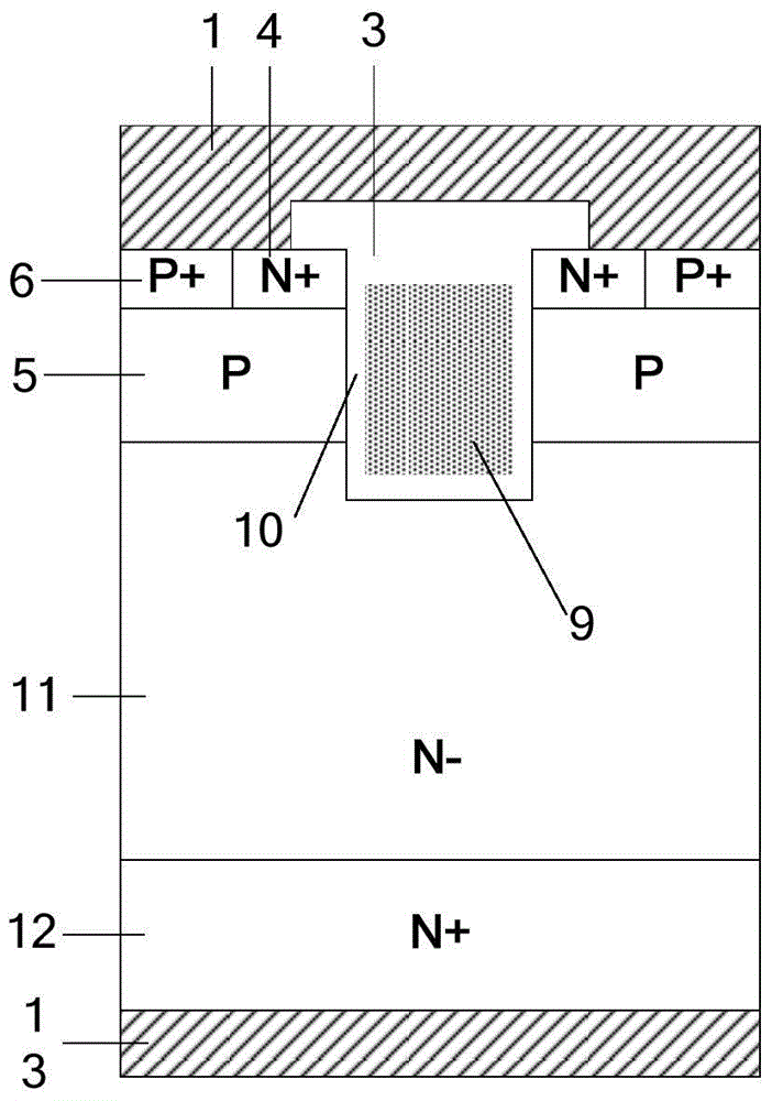
A trench-gate vdmos device with integrated schottky diode
A Schottky diode and Schottky junction technology, applied in the direction of diodes, semiconductor devices, electrical components, etc., can solve the problem of poor switching characteristics of VDMOS devices, poor reverse recovery characteristics, high stored charge diode peak reverse current, etc. question
- Summary
- Abstract
- Description
- Claims
- Application Information
AI Technical Summary
Problems solved by technology
Method used
Image
Examples
Embodiment 1
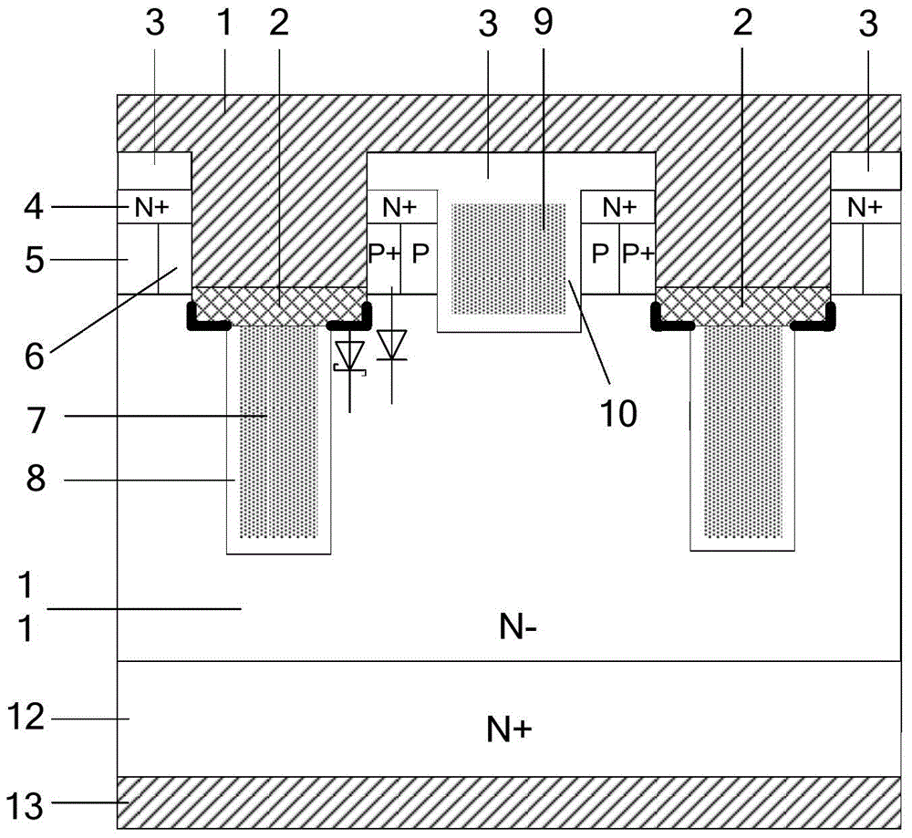
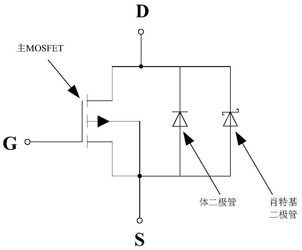
[0032] figure 2 It shows a specific embodiment of the groove gate VDMOS device integrating Schottky diodes proposed by the present invention, including: a highly doped semiconductor substrate 12 of the first conductivity type, and a back contact with the semiconductor substrate 12 of the highly doped first conductivity type The drain metal 13 and the low-doped first-conductivity-type semiconductor drift region 11 in front contact with the highly-doped first-conductivity-type semiconductor substrate 12; A second conductivity type semiconductor body region 5, in each second conductivity type semiconductor body region 5 has a highly doped first conductivity type semiconductor source region 4 and a highly doped second conductivity type semiconductor body contact region 6 which are independent of each other , the surfaces of the highly doped first conductivity type semiconductor source region 4 and the highly doped second conductivity type semiconductor body contact region 6 are i...
Embodiment 2
[0047] Such as Figure 6.1 As shown, compared with Embodiment 1, the process of Embodiment 2 is generally the same, except that a second layer of low-doped first-conductivity-type semiconductor is added to the surface of the low-doped first-conductivity-type semiconductor drift region 11 (the first epitaxial layer). Epitaxial layer 15.
[0048] According to needs, the turn-on voltage and withstand voltage of the Schottky diode can be adjusted by adjusting the concentration of the second epitaxial layer 15, and adjusting the concentration will also slightly affect the forward conduction characteristics of the device, reducing the doping of the second epitaxial layer 15 Concentration can increase the withstand voltage of the Schottky junction, but at the same time it will increase the resistance of the drift region, which will slightly increase the conduction voltage drop, and a compromise design can be made according to the specific situation.
Embodiment 3
[0050] Such as Figure 6.2 As shown, compared with Embodiment 1, the polysilicon gate electrode 10 and the polysilicon body electrodes 7 on both sides adopt the same trench depth in Embodiment 3.
[0051] Using the same trench depth, the gate electrode trench and the body electrode trenches on both sides can be formed in the same etching process, which can reduce the etching process steps; in addition, this design can optimize the forward resistance more effectively. The electric field distribution in the off-time drift region is because mutual protection can be formed between the grooves from the top of the groove to the bottom where the electric field lines are densest, and the locally concentrated electric field lines are dispersed, and the withstand voltage of the device can be further improved.
PUM
 Abstract
Description
Claims
Application Information
 - R&D
- Intellectual Property
- Life Sciences
- Materials
- Tech Scout
- Unparalleled Data Quality
- Higher Quality Content
- 60% Fewer Hallucinations
Browse by: Latest US Patents, China's latest patents, Technical Efficacy Thesaurus, Application Domain, Technology Topic, Popular Technical Reports.
© 2025 PatSnap. All rights reserved.Legal|Privacy policy|Modern Slavery Act Transparency Statement|Sitemap|About US| Contact US: help@patsnap.com


