Double patterning method in back-end-of-line

A double patterning, back-end process technology, applied in the field of integrated circuit manufacturing, can solve the problems of difficult application of double patterning technology, and achieve the effect of reducing etching damage, avoiding etching process, and protecting dielectric capability.

Active Publication Date: 2013-12-04
SEMICON MFG INT (SHANGHAI) CORP
View PDF6 Cites 10 Cited by
  • Summary
  • Abstract
  • Description
  • Claims
  • Application Information

AI Technical Summary

Problems solved by technology

[0006] However, in the semiconductor back-end process (BEOL, Back End of Line), the formed interconnection metal lines have a large number of corner patterns, such as 90-degree corners, making it difficult to apply the self-aligned double patterning technology to the back-end process. middle
The method of forming double patterning in the semiconductor back-end process faces great technical challenges

Method used


Image

  • Double patterning method in back-end-of-line
  • Double patterning method in back-end-of-line
  • Double patterning method in back-end-of-line

Examples


Embodiment Construction

[0030] In order to make the content of the present invention clearer and easier to understand, the content of the present invention will be further described below in conjunction with the accompanying drawings. Of course, the present invention is not limited to this specific embodiment, and general replacements known to those skilled in the art are also covered within the protection scope of the present invention.

[0031] Secondly, the present invention is described in detail by means of schematic diagrams. When describing the examples of the present invention in detail, for the convenience of explanation, the schematic diagrams are not partially enlarged according to the general scale, which should not be used as a limitation of the present invention.

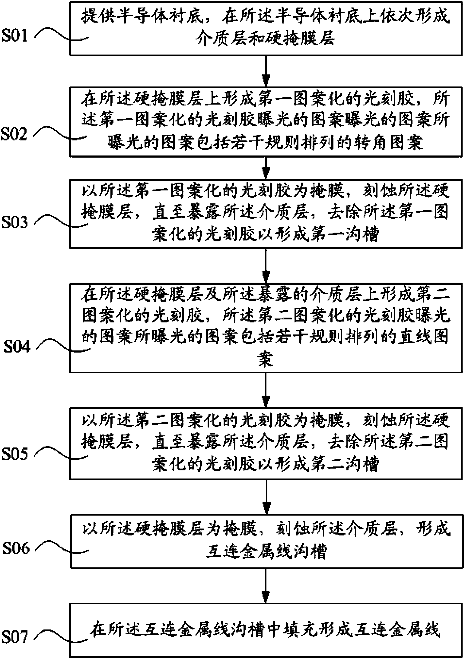
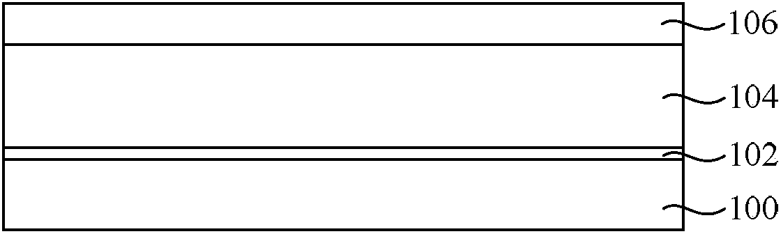
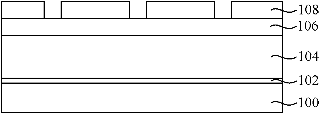
[0032] figure 1 It is a schematic flowchart of a double patterning method in a back-end process in an embodiment of the present invention. Such as figure 1 As shown, the present invention provides a double patterning method...


PUM

PropertyMeasurementUnit
thicknessaaaaaaaaaa

Abstract

The invention provides a double patterning method in a back-end-of-line. The double patterning method in the back-end-of-line comprises the steps of forming a medium layer and a hard mask layer on a semiconductor substrate in sequence; forming first patterning optical resist, wherein patterns exposed by the first patterning optical resist comprise a plurality of turn angle patterns arranged regularly; etching the hard mask layer to formed a first groove; forming second patterning optical resist, wherein patterns exposed by the second patterning optical resist comprise a plurality of straight line patterns arranged regularly; etching the hard mask layer to form a second groove; etching the medium layer to form interconnected metal wire grooves with the hard mask layer taken as a mask; carrying out stuffing on the interconnected metal wire grooves to form interconnected metal wires. According to the double patterning method in the back-end-of-line, error size alignment can be carried out more easily, and therefore alignment precision in the back-end-of-line with the turn angle patterns can be improved.

Description

technical field [0001] The invention relates to the field of integrated circuit manufacturing, in particular to a double patterning method in the back-end process. Background technique [0002] With the increasing integration of semiconductor devices, the volume and critical dimension (Critical Dimension) of semiconductor devices continue to shrink, and the critical dimension gradually approaches or even exceeds the physical limit of optical lithography. The integrated circuit industry, especially lithography technology, is facing more severe challenges. The industry has been committed to prolonging the life of chemical lithography platforms, and various resolution enhancement technologies and optical proximity correction technologies have been widely used in the industry. [0003] Lithography resolution enhancement technologies such as double patterning, double exposure, high refractive index immersion, and extreme ultraviolet lithography (EUV) are expected to achieve tech...

Claims


Application Information

Patent Timeline
Patent Type & Authority Applications(China)
IPC IPC(8): H01L21/768G03F1/76
Inventor 符雅丽王新鹏张海洋
Owner SEMICON MFG INT (SHANGHAI) CORP
Why Eureka
Try Eureka