Detection circuit and detection method of bias temperature instability
A technology of instability and bias temperature, applied in the direction of electronic circuit testing, etc., can solve problems such as the influence of oscillation frequency and threshold voltage degradation, and achieve the effect of high precision and amplified detection results
- Summary
- Abstract
- Description
- Claims
- Application Information
AI Technical Summary
Problems solved by technology
Method used
Image
Examples
no. 1 example
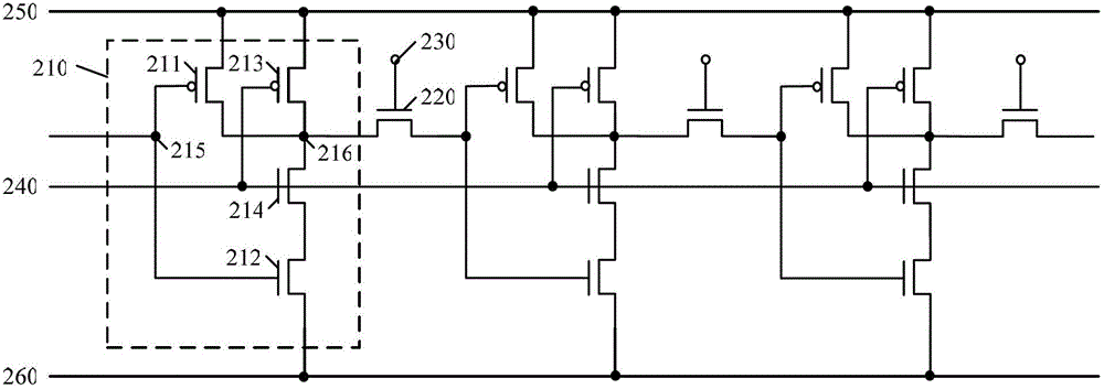
[0041] The first embodiment of the present invention firstly provides a detection circuit for detecting the temperature instability of the positive bias voltage of the NMOS transistor, please refer to figure 2 , is a schematic structural diagram of a detection circuit for bias temperature instability in an embodiment of the present invention, specifically including:
[0042] An odd number of basic oscillation units 210 with the same circuit structure, wherein the basic oscillation unit 210 includes a first transistor 211, a second transistor 212, a first control transistor 213, a second control transistor 214, an input terminal 215, and an output terminal 216. A transistor 211 and the first control transistor 213 are PMOS transistors, and the second transistor 212 and the second control transistor 214 are NMOS transistors;
[0043] The gates of the first transistor 211 and the second transistor 212 are connected to the input terminal 215, the gates of the first control transi...
no. 2 example
[0067] The second embodiment of the present invention provides a detection circuit for detecting the temperature instability of the negative bias voltage of the PMOS transistor, please refer to Figure 4 , is a schematic structural diagram of a detection circuit for bias temperature instability in an embodiment of the present invention, specifically including:
[0068] An odd number of basic oscillation units 310 with the same circuit structure, wherein the basic oscillation unit 310 includes a first transistor 311, a second transistor 312, a first control transistor 313, a second control transistor 314, an input terminal 315, and an output terminal 316. A transistor 311 and the first control transistor 313 are NMOS transistors, and the second transistor 312 and the second control transistor 314 are PMOS transistors;
[0069] The gates of the first transistor 311 and the second transistor 312 are connected to the input terminal 315, the gates of the first control transistor 31...
PUM
 Abstract
Description
Claims
Application Information
 - R&D
- Intellectual Property
- Life Sciences
- Materials
- Tech Scout
- Unparalleled Data Quality
- Higher Quality Content
- 60% Fewer Hallucinations
Browse by: Latest US Patents, China's latest patents, Technical Efficacy Thesaurus, Application Domain, Technology Topic, Popular Technical Reports.
© 2025 PatSnap. All rights reserved.Legal|Privacy policy|Modern Slavery Act Transparency Statement|Sitemap|About US| Contact US: help@patsnap.com


