


Quick Research
Generate reliable direction feasibility study reports for your R&D in just a few steps.

Technical Q&A
Discover and master advanced knowledge NOW. Basics, ideas, possibilities, all at once.

Find Solutions
As an expert in R&D theories, this can generate solutions to your technical problems instantly.

Evaluate Feasibility
Analyze your overall solution with one click, know your potential R&D risks in advance.

Monitor Landscape
Get weekly tech updates, stay abreast of the latest tech innovations and key insights.
pmos transistor and its forming method
A technology of transistors and semiconductors, applied in semiconductor devices, semiconductor/solid-state device manufacturing, electrical components, etc., can solve the problems of small increase in carrier mobility, limited improvement in transistor performance, and limited stress, so as to improve electrical performance, Effects of suppression of decrease in threshold voltage and uniformity of compressive stress
- Summary
- Abstract
- Description
- Claims
- Application Information
AI Technical Summary
Problems solved by technology
Method used
Image


Examples
Embodiment Construction
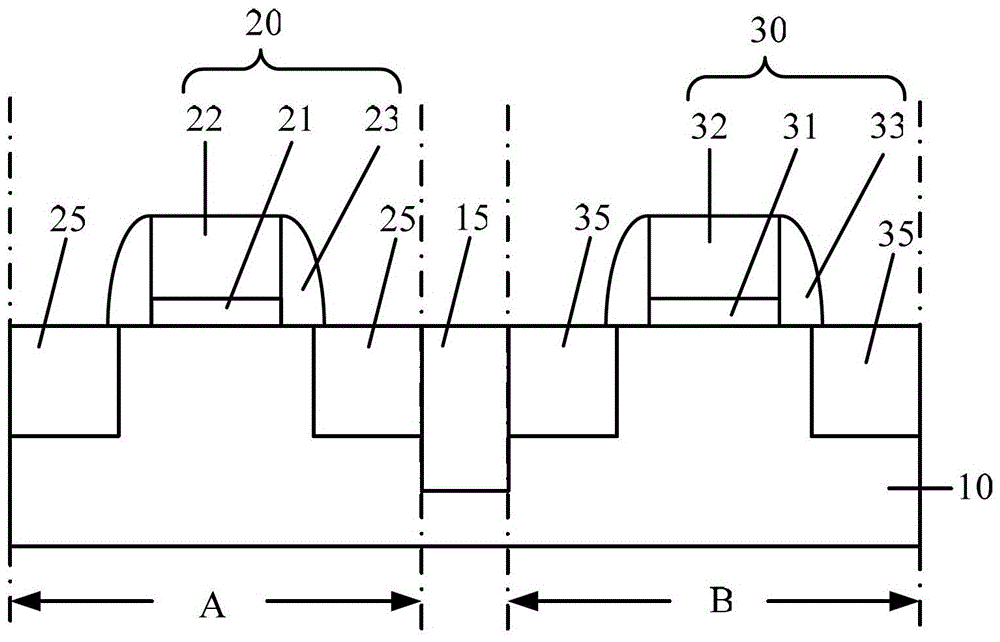
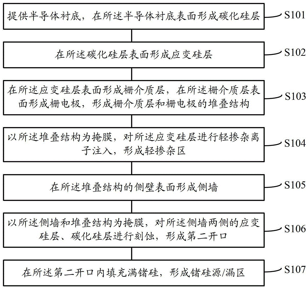
[0047] Due to the limited stress generated by the silicon germanium source / drain region or silicon carbide source / drain region of the MOS transistor in the prior art to the channel region under the gate structure, the improvement of the carrier mobility is small, and the performance of the transistor is improved. limited. For this reason, the inventor proposes a PMOS transistor and its forming method. The forming method of the PMOS transistor includes: providing a semiconductor substrate, forming a silicon carbide layer on the surface of the semiconductor substrate; forming a strain on the surface of the silicon carbide layer. A silicon layer; a gate structure is formed on the surface of the strained silicon layer; and silicon germanium source / drain regions are formed in the silicon carbide layer on both sides of the gate structure. Since the channel region of the PMOS transistor in the embodiment of the present invention is located in the silicon carbide layer and the straine...
PUM
| Property | Measurement | Unit |
|---|---|---|
| thickness | aaaaa | aaaaa |
| thickness | aaaaa | aaaaa |
| thickness | aaaaa | aaaaa |
Abstract
Description
Claims
Application Information
 - R&D Engineer
- R&D Manager
- IP Professional
- Industry Leading Data Capabilities
- Powerful AI technology
- Patent DNA Extraction
Browse by: Latest US Patents, China's latest patents, Technical Efficacy Thesaurus, Application Domain, Technology Topic, Popular Technical Reports.
© 2024 PatSnap. All rights reserved.Legal|Privacy policy|Modern Slavery Act Transparency Statement|Sitemap|About US| Contact US: help@patsnap.com