


Quick Research
Generate reliable direction feasibility study reports for your R&D in just a few steps.

Technical Q&A
Discover and master advanced knowledge NOW. Basics, ideas, possibilities, all at once.

Find Solutions
As an expert in R&D theories, this can generate solutions to your technical problems instantly.

Evaluate Feasibility
Analyze your overall solution with one click, know your potential R&D risks in advance.

Monitor Landscape
Get weekly tech updates, stay abreast of the latest tech innovations and key insights.
TSV hole bottom medium layer etching method
A dielectric layer, all technologies, applied in the field of microelectronics, can solve the problems of increasing the difficulty of etching, damage to the insulating layer material of the sidewall of the TSV hole, etc.
- Summary
- Abstract
- Description
- Claims
- Application Information
AI Technical Summary
Problems solved by technology
Method used
Image

Examples
Embodiment 1
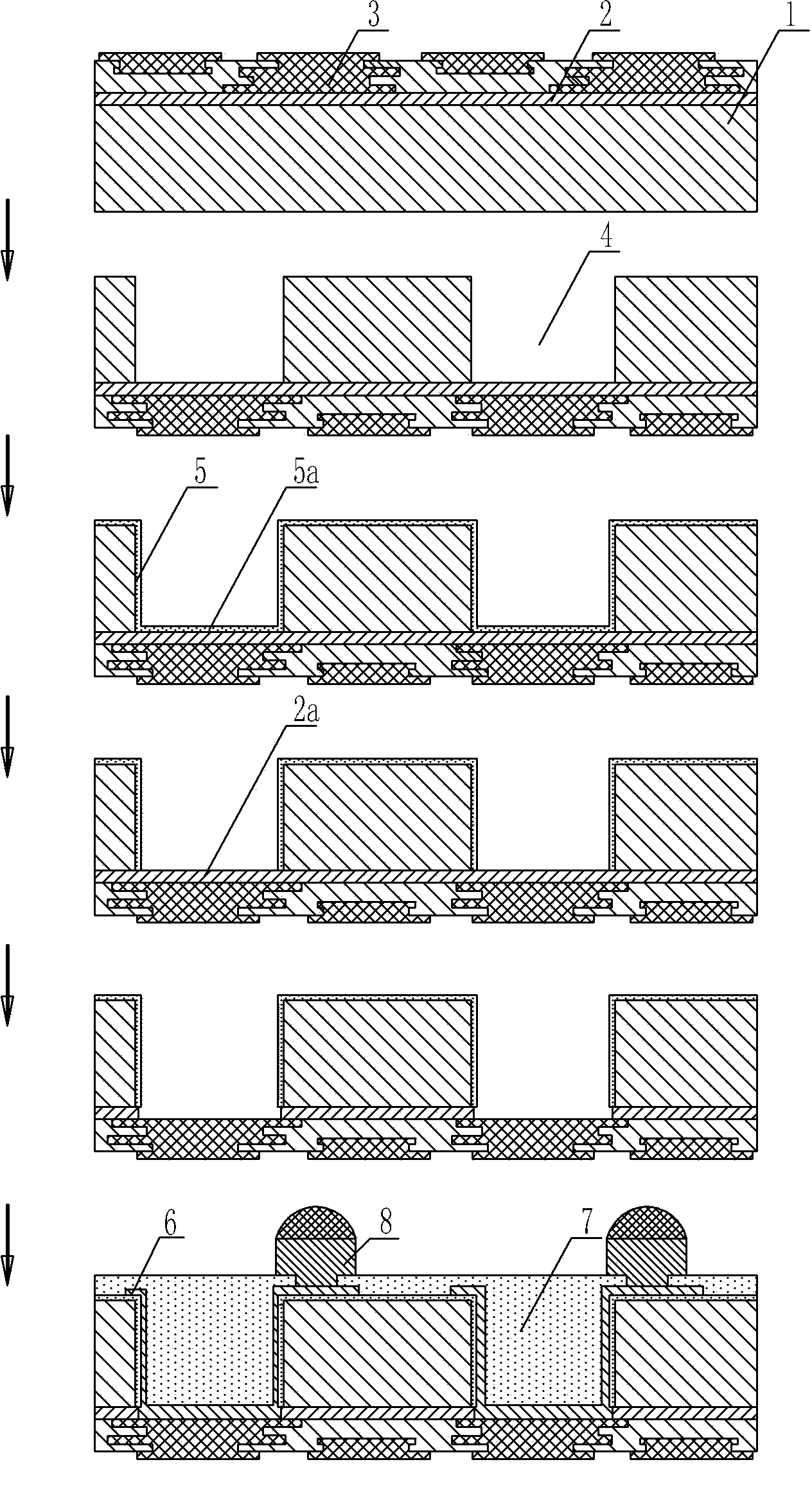
[0026] (1) Thinning the backside of an 8-inch, 725um-thick wafer 1 with IC devices;
[0027] A: There is a metal pad 3 inside the IC device wafer, and there is an oxide insulating layer 2 with a thickness of 1.5um between the metal pad and the IC device;
[0028] B: Use a wafer thinning machine to thin the back side of the IC device wafer 1, so that the wafer is thinned to 100um;
[0029] (2) Fabricate TSV holes 4 at the positions corresponding to the metal pads on the back of the IC device wafer 1; from the back of the wafer, fabricate TSV holes 4 by deep reactive ion etching at the position facing the metal pads 3, The aperture is 24um, when etching the TSV hole, until the oxide insulating layer 2 above the metal pad is fully exposed;
[0030] (3) Make a polymer insulating layer 5 in the TSV hole 4; make a 2um polymer insulating layer 5 on the side wall and bottom of the TSV hole by spin coating or spraying, and the polymer material is PI;
[0031] (4) Remove the polymer i...
Embodiment 2
[0035] (1) Thinning the backside of an 8-inch, 725um-thick wafer 1 with IC devices;
[0036] A: There is a metal pad 3 inside the IC device wafer, and there is an oxide insulating layer 2 with a thickness of 1.5um between the metal pad and the IC device;
[0037] B: Use a wafer thinning machine to thin the back side of the IC device wafer 1, so that the wafer is thinned to 120um;
[0038] (2) Fabricate TSV holes 4 at the positions corresponding to the metal pads on the back of the IC device wafer 1; from the back of the wafer, fabricate TSV holes 4 by deep reactive ion etching at the position facing the metal pads 3, The aperture is 36um, when etching the TSV hole 4, until the oxide insulating layer 2 above the metal pad is fully exposed;
[0039] (3) Make a polymer insulating layer 2 in the TSV hole; make a 3.5um polymer insulating layer 5 on the side wall and bottom of the TSV hole by spin coating or spraying, and the polymer material is PI;
[0040] (4) Remove the polymer...
Embodiment 3
[0044] (1) Thinning the backside of an 8-inch, 725um-thick wafer 1 with IC devices;
[0045] A: There is a metal pad 3 inside the IC device wafer, and there is an oxide insulating layer 2 with a thickness of 2um between the metal pad and the IC device;
[0046] B: Use a wafer thinning machine to thin the back of IC device wafer 1, so that the wafer is thinned to 150um;
[0047] (2) Make TSV holes 4 at the positions corresponding to the metal pads 3 on the back of the IC device wafer 1; from the back of the wafer, make TSV holes 4 at the positions facing the metal pads 3 by deep reactive ion etching , the aperture is 50um, when etching the TSV hole 4, until the oxide insulating layer 2 above the metal pad 3 is fully exposed;
[0048] (3) Make a polymer insulating layer 5 in the TSV hole 4; make a 5um polymer insulating layer 5 on the side wall and bottom of the TSV hole by spin coating or spraying, and the polymer material is PBO;
[0049] (4) Remove the polymer insulating laye...
PUM
 Abstract
Description
Claims
Application Information
 - R&D Engineer
- R&D Manager
- IP Professional
- Industry Leading Data Capabilities
- Powerful AI technology
- Patent DNA Extraction
Browse by: Latest US Patents, China's latest patents, Technical Efficacy Thesaurus, Application Domain, Technology Topic, Popular Technical Reports.
© 2024 PatSnap. All rights reserved.Legal|Privacy policy|Modern Slavery Act Transparency Statement|Sitemap|About US| Contact US: help@patsnap.com