Method for preparing supersaturated-doping semiconductor thin film

A semiconductor and thin film technology, which is applied in the field of supersaturated doped semiconductor thin film preparation, can solve problems such as inhomogeneity, unfavorable device production and performance, and uneven distribution of sulfur atom concentration, so as to achieve favorable device performance and uniform doping concentration. Effect

Inactive Publication Date: 2013-08-28
INST OF SEMICONDUCTORS - CHINESE ACAD OF SCI
View PDF7 Cites 7 Cited by
  • Summary
  • Abstract
  • Description
  • Claims
  • Application Information

AI Technical Summary

Problems solved by technology

But its disadvantage is that the concentration distribution of doped sulfur atoms in the implanted layer is very uneven. This is because the concentration distribution of dopant atoms in the semiconductor after ion implantation is a Gaussian distribution, and it is also very uneven after ultrafast laser annealing. , which adversely affects the fabrication and performance of the device

Method used


Image

  • Method for preparing supersaturated-doping semiconductor thin film

Examples


Embodiment Construction

[0012] In order to make the object, technical solution and advantages of the present invention clearer, the present invention will be further described in detail below in conjunction with specific embodiments and with reference to the accompanying drawings.

[0013] The invention provides a method for preparing a supersaturated doped semiconductor thin film.

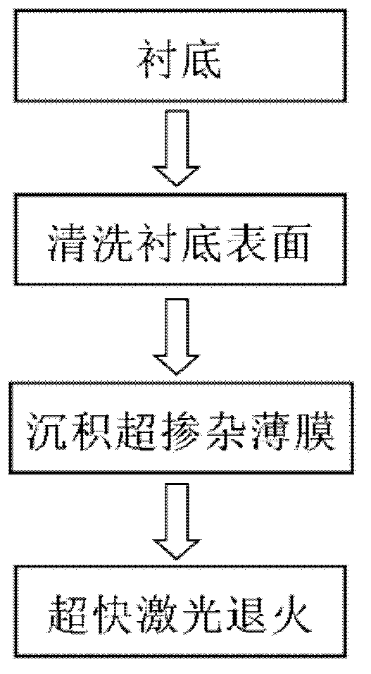
[0014] figure 1 The flow chart of the preparation method of the supersaturated doped semiconductor thin film proposed by the present invention is shown. Such as figure 1 As shown, the method includes the following steps:

[0015] Step 1: Select a substrate. The material of the substrate can be various types of semiconductor substrates. In this example, a silicon single wafer is selected, and its crystal plane orientation is (001), and both sides are polished, p-type boron doped, and the resistivity between 1~10Ωcm, the thickness of wafer is 390±20μm;

[0016] Step 2: Rotate and clean the substrate three times in tric...


PUM

PropertyMeasurementUnit
thicknessaaaaaaaaaa

Abstract

The invention discloses a method for preparing a supersaturated-doping semiconductor thin film. The method includes the following steps: step one, a substrate is chosen; step two, the surface of the substrate is cleaned up; step three, at a low growth temperature, a semiconductor amorphous thin film is deposited on the surface of the substrate, wherein through control over a deposition speed ratio of atoms, a supersaturated-doping semiconductor amorphous thin film is obtained; step four, laser annealing is carried out on the supersaturated-doping semiconductor amorphous thin film by the utilization of ultra-fast lasers, and the preparation of the supersaturated-doping semiconductor thin film is completed. According to the preparation method, the molecular beam epitaxy technology is used for preparing the supersaturated-doping thin film which is even in doping concentration. Depth distribution of impurities in the prepared supersaturated-doping silicon thin film is very even.

Description

technical field [0001] The invention belongs to the field of semiconductor thin film materials, and in particular relates to a preparation method of a supersaturated doped semiconductor thin film. Background technique [0002] In recent years, there has been intense research interest in supersaturated doped semiconductor materials. The so-called supersaturated doped semiconductor material means that the doping concentration of the dopant inside the semiconductor material has begun to exceed its thermodynamic equilibrium solubility. If a semiconductor material is doped with a deep-level impurity, the dopant atoms can form an impurity state within the forbidden band of the semiconductor material. In this case, as the concentration of dopant atoms increases, the isolated impurity states can be coupled with each other, and finally impurity bands are formed, which is the so-called intermediate band semiconductor material. Inserting an intermediate band inside common semiconduct...

Claims


Application Information

Patent Timeline
Patent Type & Authority Applications(China)
IPC IPC(8): H01L21/02
Inventor 王科范张华荣彭成晓曲胜春王占国
Owner INST OF SEMICONDUCTORS - CHINESE ACAD OF SCI
Why Eureka
Try Eureka