
Gate-grounded NMOS manufacturing method

A manufacturing method, semiconductor technology, applied in semiconductor/solid-state device manufacturing, electrical components, circuits, etc.

Active Publication Date: 2013-07-03
SEMICON MFG INT (SHANGHAI) CORP
View PDF5 Cites 2 Cited by
  • Summary
  • Abstract
  • Description
  • Claims
  • Application Information

AI Technical Summary

Problems solved by technology

[0007] Since the ESD implantation dose is much larger than the LDD implantation, there is a problem of lateral diffusion, so the leakage problem and the parasitic capacitance problem must be considered.

Method used


Image

  • Gate-grounded NMOS manufacturing method

Examples


Embodiment Construction

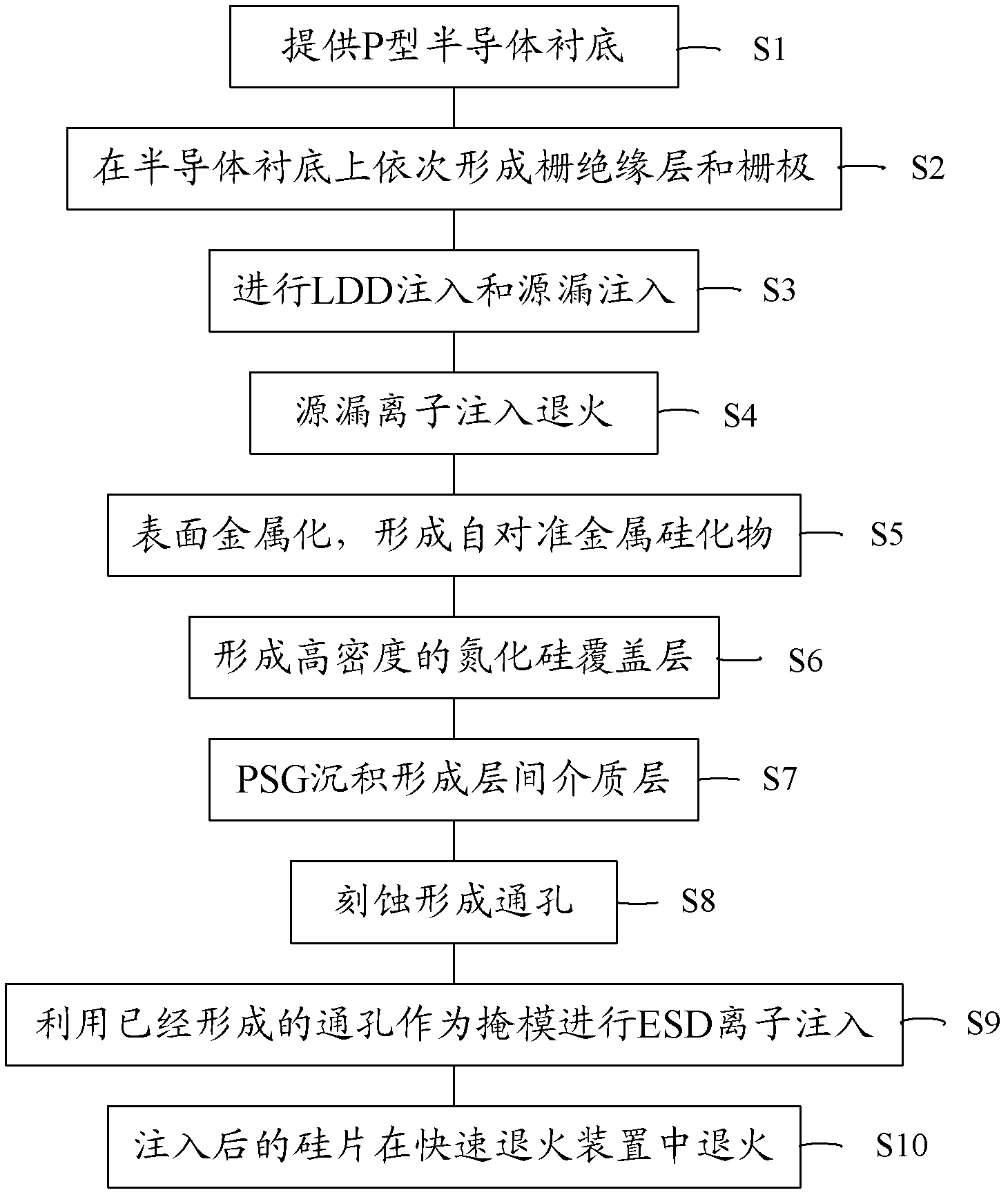
[0026] The present invention uses ESD Implant in the contact hole after the contact hole is formed on the source and drain and before filling the metal plug, which reduces the steps of the original process, reduces the area of ​​the ESD Implant in the drain, and improves the static electricity of the GGNMOS. protective properties.

[0027] The concrete steps that the present invention makes GGNMOS include:

[0028] Step S1: providing a P-type semiconductor substrate;

[0029] Step S2: sequentially forming a gate insulating layer and a gate on the semiconductor substrate;

[0030] Step S3: performing LDD injection and source-drain injection;

[0031] Step S4: source-drain ion implantation annealing;

[0032] Step S5: Surface metallization to form salicide;

[0033] Step S6: forming a high-density silicon nitride capping layer;

[0034] Step S7: PSG is deposited to form an interlayer dielectric layer;

[0035] Step S8: etching to form a through hole;

[0036] Step S9: per...


PUM


Abstract

The invention relates to a gate-grounded NMOS (GGNMOS) manufacturing method which includes the following steps. A P-shaped semi-conductor substrate is provided. A gate insulation layer and a grid electrode are sequentially formed on the semi-conductor substrate, source drain implantation is performed, an interlamination medium layer is formed, a through hole of a contact hole is formed in an etching mode and ESD ion filling is performed by using the formed through hole as a reticle mask. Compared with that ESD filling is performed before the contact hole is formed in manufacturing the GGNMOS, performing the ESD filling after the through hole of the contact hole is formed can not only reduce procedures of original technology, narrow down an ESD Implant zone in a drain electrode and reduce leakage, but also reduce grid leak parasitic capacitance caused by horizontal spreading and improve static protection characteristics of the GGNMOS.

Description

technical field [0001] The invention relates to the field of semiconductor manufacturing, in particular to a method for manufacturing GGNMOS (Gate Grounded NMOS, N-type metal oxide transistor with a gate grounded). Background technique [0002] Integrated circuits are easily damaged by static electricity. Generally, electrostatic protection circuits are designed at the input and output terminals of the circuit or power protection devices to prevent internal circuits from being damaged by static electricity. GGNMOS (Gate Grounded NMOS, gate grounded N-type metal oxide transistor) is a widely used electrostatic protection structure. It performs electrostatic protection through electrostatic discharge. The mechanism is: since the power consumption on the MOS tube is the product of the passing current and the voltage drop, under a certain ESD electrostatic current, if the voltage drop on it can be reduced, the MOS tube can be reduced. The power consumption on the tube, thereby ...

Claims


Application Information

Patent Timeline
IPC IPC(8): H01L21/336
Inventor 赵猛
Owner SEMICON MFG INT (SHANGHAI) CORP
Learn More