LDMOS (Laterally Diffused Metal Oxide Semiconductor) with selective shallow slot through hole and production method thereof

A selective, shallow trench technology, applied in the structure and preparation of LDMOS, can solve the problems of easy damage, lower reliability of LDMOS, lower reverse breakdown voltage of LDMOS, etc., achieve large process window, reduce design size and The effect of chip area and reliability risk reduction

Inactive Publication Date: 2013-06-26
SHANGHAI HUAHONG GRACE SEMICON MFG CORP
View PDF5 Cites 2 Cited by
  • Summary
  • Abstract
  • Description
  • Claims
  • Application Information

AI Technical Summary

Problems solved by technology

[0006] Due to the limitations of photolithography and implantation process, when the source / drain end implantation process of LDMOS is performed, the pattern defining the same-type doped region as the body region will be small, and the photoresist in this region (such as figure 2 (indicated by the arrow in the middle) is easily damaged. If the photoresist is damaged, the body region of the LDMOS cannot be drawn out, and it is short-circuited with the source terminal, such as image 3 As shown, in this way, the parasitic BJT will reduce the reverse breakdown voltage of LDMOS, reduce the SOA of LDMOS, and then lead to a decrease in the reliability of LDMOS

Method used


Image

  • LDMOS (Laterally Diffused Metal Oxide Semiconductor) with selective shallow slot through hole and production method thereof
  • LDMOS (Laterally Diffused Metal Oxide Semiconductor) with selective shallow slot through hole and production method thereof
  • LDMOS (Laterally Diffused Metal Oxide Semiconductor) with selective shallow slot through hole and production method thereof

Examples


Embodiment Construction

[0026] In order to have a more specific understanding of the technical content, characteristics and effects of the present invention, now in conjunction with the illustrated embodiment, the details are as follows:

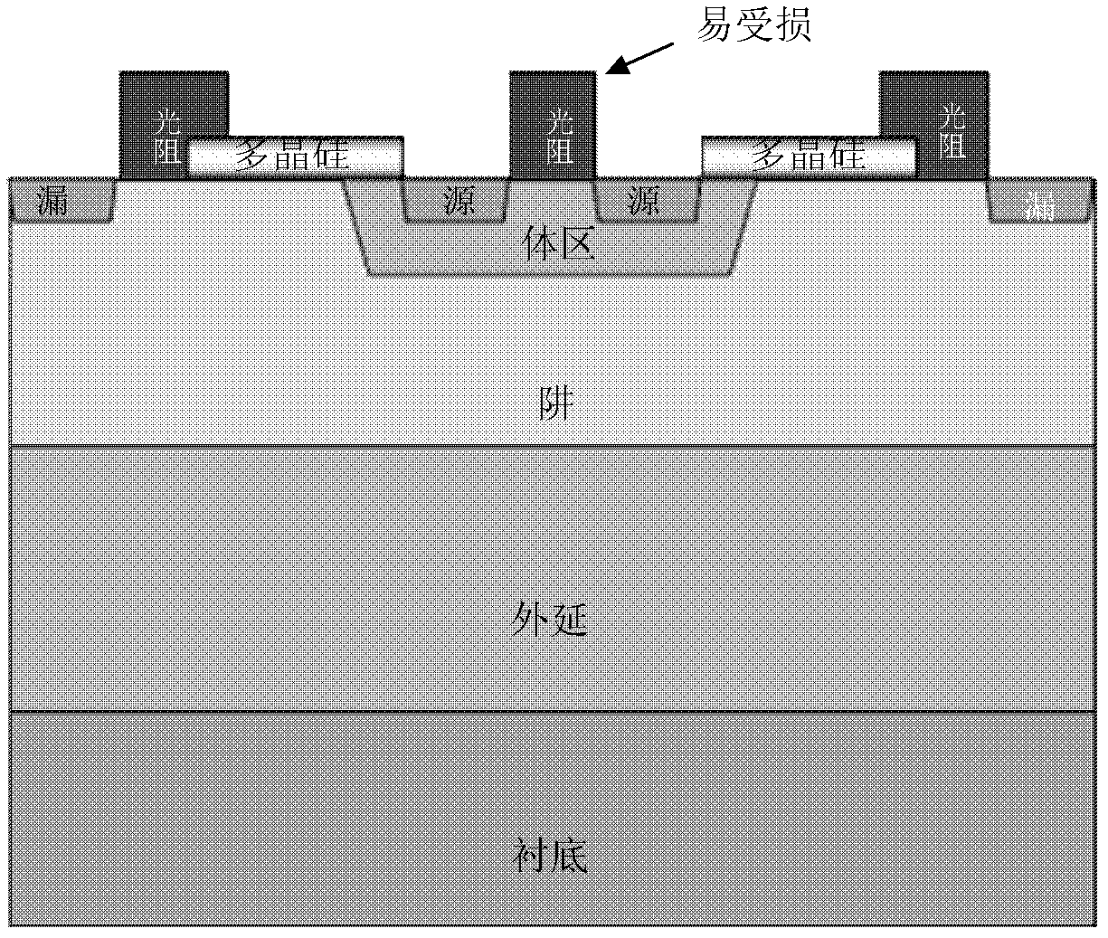
[0027] The selective shallow trench via technology uses different etching rates for different materials to form shallow trench vias in specific areas while forming normal vias in other areas. In this embodiment, the selective shallow trench via technology is applied, and the LDMOS with selective shallow trench via is developed according to the following preparation process:

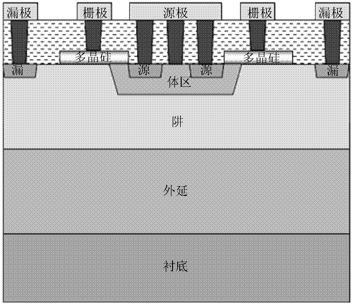
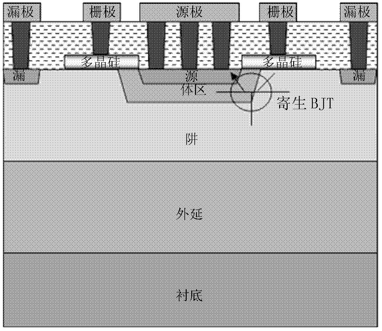
[0028] Step 1, grow an epitaxial layer on a silicon substrate, make a well on the epitaxial layer, deposit a layer of polysilicon, etch to form a gate, and then form a body region, a source region, and a drain region (no need to define homotype doping with the body region region), complete the front-end preparation process of LDMOS semiconductor, and form the basic structure of LDMOS, such as ...


PUM


Abstract

The invention discloses a production method of an LDMOS (Laterally Diffused Metal Oxide Semiconductor) with a selective shallow slot through hole. The production method of an LDMOS with a selective shallow slot through hole comprises forming a basic structure, forming bottom layer interlamination film; forming a blocking layer; etching the blocking layer which is arranged in an area of the shallow slot through hole; forming top layer interlamination film; performing multi-step high selective etching to form a normal through hole in an area of the blocking layer and the shallow slot through hole of a connector area in an area without the blocking layer; and injecting doping source which has the same type with the connector area at the bottom of the shallow slot through hole after a basic structure is formed. The invention also discloses an LDMOS structure which is produced through the production method. The production method of the LDMOS with the selective shallow slot through hole has the advantages of effectively reducing design size of a source end and an area of a chip and improving reliability of a component due to the fact that different types of doping areas which are vertically distributed in a specified area of the LDMOS are connected with each other with the help of a selective shallow slot through hole technology.

Description

technical field [0001] The invention relates to the field of semiconductor integrated circuit manufacturing, in particular to an LDMOS structure with selective shallow trench through holes and a preparation method thereof. Background technique [0002] Laterally Diffused Metal Oxide Semiconductor (LDMOS) devices have been widely used in mobile communication fields such as CDMA due to their good compatibility with CMOS processes. [0003] A typical LDMOS device structure is as figure 1 As shown, the LDMOS has a parasitic bipolar transistor (BJT) composed of drain-body-well. Once the parasitic BJT works, the reverse breakdown voltage of the LDMOS will be reduced to the emitter of the parasitic BJT. -Collector breakdown voltage; In addition, due to the secondary breakdown effect of BJT, LDMOS will also undergo secondary breakdown, which will reduce the safe operating area (SOA). These two problems will lead to a decrease in the reliability of LDMOS . [0004] In order to sol...

Claims


Application Information

Patent Timeline
Patent Type & Authority Applications(China)
IPC IPC(8): H01L21/336H01L29/78
Inventor 王星杰
Owner SHANGHAI HUAHONG GRACE SEMICON MFG CORP
Why Eureka
Try Eureka