Preparation method for gas-sensitive material with composite structure
A gas-sensitive material and composite structure technology, which is applied in the field of preparation of porous silicon-based tungsten oxide composite structure gas-sensitive materials, and achieves the effects of easy control of process parameters, convenient operation and low cost
- Summary
- Abstract
- Description
- Claims
- Application Information
AI Technical Summary
Problems solved by technology
Method used
Image
Examples
Embodiment 1
[0032] (1) Clean the silicon substrate
[0033] Cut a 2-inch n-type single-sided polished single-crystal silicon wafer with a resistivity of 0.01Ω·cm, a thickness of 400μm, and (100) crystal orientation into rectangular silicon substrates with a size of 2.4cm×0.9cm, and put them in acetone in turn Solvent, absolute ethanol and deionized water were ultrasonically cleaned for 20 minutes, and then soaked in 5% hydrofluoric acid aqueous solution for 15 minutes, and then washed with deionized water for later use;
[0034] (2) Preparation of porous silicon
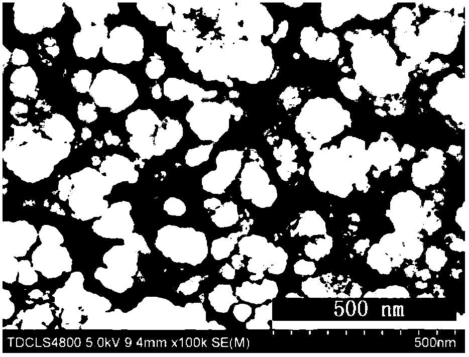
[0035] A porous silicon layer was prepared on the polished surface of a silicon wafer by a double-tank electrochemical method. The corrosion electrolyte used is composed of hydrofluoric acid and deionized water with a mass fraction of 40%, the volume ratio is 1:5, no surfactant and additional light are added, and the applied corrosion current density is 125mA / cm 2 , the etching time is 20min; wherein the porous silicon formati...
Embodiment 2
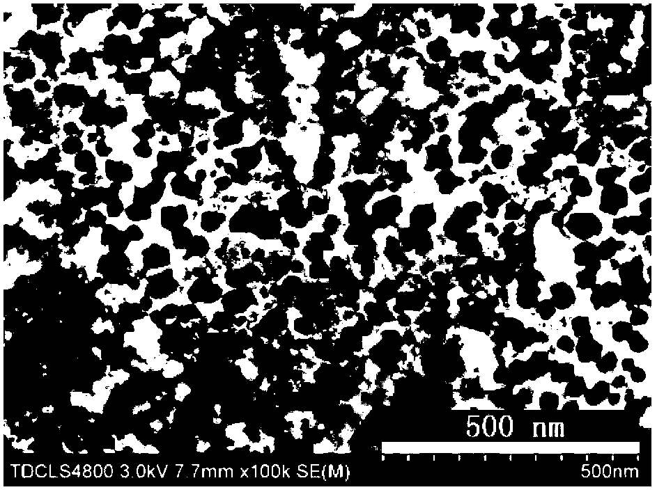
[0040] The difference between this example and Example 1 is that the sputtering time of the tungsten oxide nano-film in step (3) is 5 minutes, and the porous silicon-based tungsten oxide composite structure gas-sensing material is prepared. Scanning electron microscopy analysis of the surface morphology showed that figure 2 As shown, the tungsten oxide film has not been uniformly covered on the surface, and there are a lot of holes.
Embodiment 3
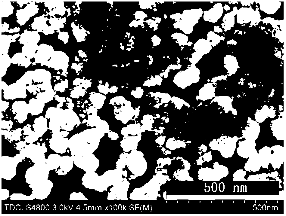
[0042] The difference between this example and Example 1 is that the sputtering time of the tungsten oxide nano-film in step (3) is 8 minutes, and the porous silicon-based tungsten oxide composite structure gas-sensing material is prepared. Scanning electron microscopy analysis of the surface morphology showed that image 3 As shown, the surface structure of the film is extremely loose, and there are a large number of deep holes.
PUM
| Property | Measurement | Unit |
|---|---|---|
| electrical resistivity | aaaaa | aaaaa |
| thickness | aaaaa | aaaaa |
| pore size | aaaaa | aaaaa |
Abstract
Description
Claims
Application Information
 - R&D
- Intellectual Property
- Life Sciences
- Materials
- Tech Scout
- Unparalleled Data Quality
- Higher Quality Content
- 60% Fewer Hallucinations
Browse by: Latest US Patents, China's latest patents, Technical Efficacy Thesaurus, Application Domain, Technology Topic, Popular Technical Reports.
© 2025 PatSnap. All rights reserved.Legal|Privacy policy|Modern Slavery Act Transparency Statement|Sitemap|About US| Contact US: help@patsnap.com


