Semiconductor nanocrystalline sensitized solar cell and preparation method thereof
A technology of solar cells and nanocrystals, applied in photosensitive devices, circuits, capacitors, etc., can solve environmental hazards, toxicity and other problems, and achieve the effects of simple preparation process, excellent photovoltaic performance, and excellent photoelectric performance of batteries
- Summary
- Abstract
- Description
- Claims
- Application Information
AI Technical Summary
Problems solved by technology
Method used
Image

Examples
Embodiment 1
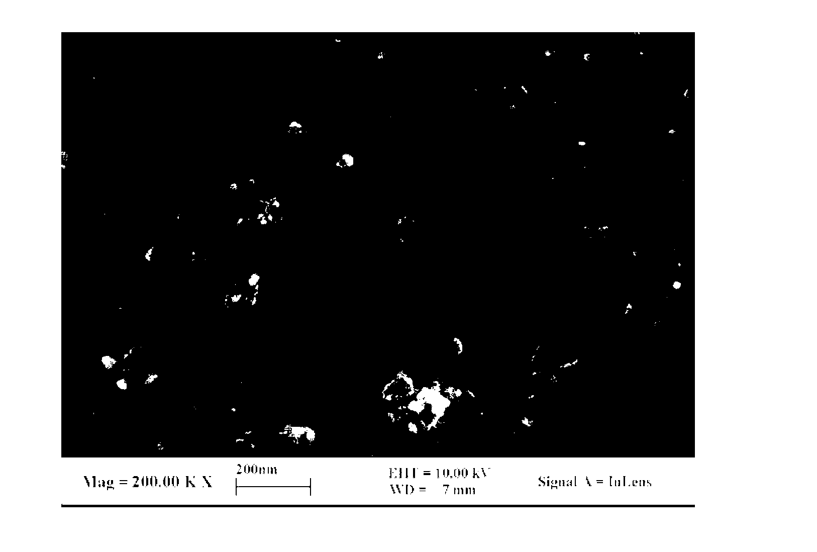
[0026] Prepare porous tin oxide film, take 5.1g SnO 2 , add an appropriate amount of ethanol and ultrasonically disperse evenly; mix 2.7 g ethyl cellulose and 12.2 g terpineol evenly, add the above SnO 2 / ethanol mixture and placed in a sonicator to disperse evenly. After the resulting mixture was placed in a rotary evaporator to remove ethanol, a uniform, viscous SnO 2 slurry. SnO 2 The slurry was placed in the screen, and after the ink was evenly covered, the film was brushed on the FTO conductive surface, and then it was left to stand for 6 minutes to make it flattened, and then placed in a 125 °C oven for heat treatment for 6 minutes. Using a field emission scanning electron microscope (LEO-1530, Germany) to observe the surface microscopic appearance of the photoanode, as figure 1 shown. The thickness of the film printed with one layer of paste is about 4 μm measured by XP-1 step tester. The FTO glass brushed with a porous film was placed in a muffle furnace and sint...
Embodiment 2
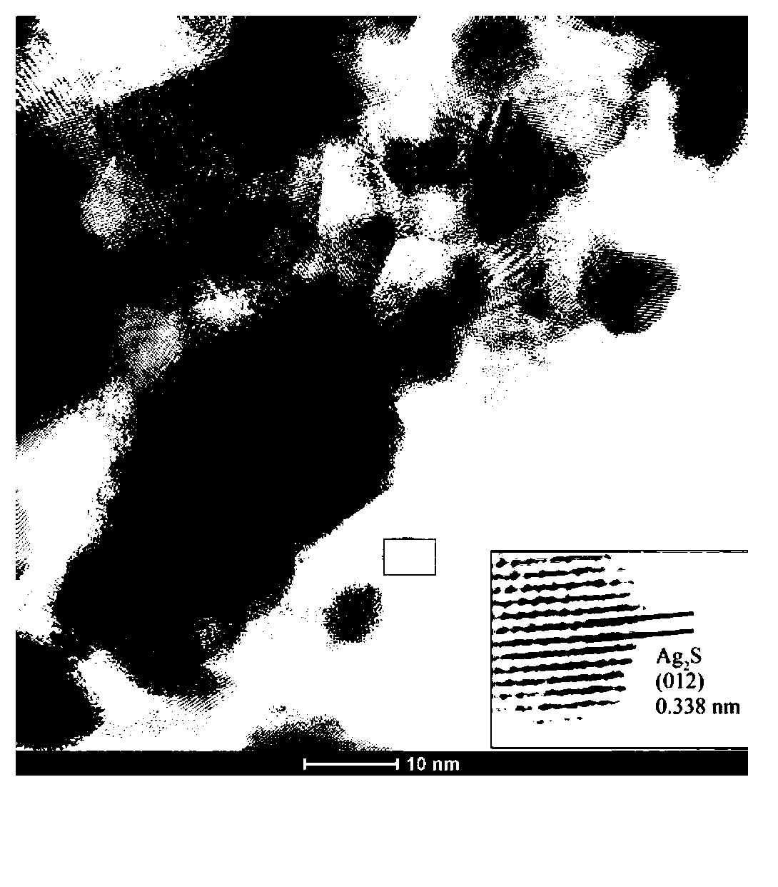
[0032] Prepare SnO with the method identical with embodiment 1 2 Slurry, screen printing 1 layer of slurry, after sintering and cooling, take out the glass and soak it in TiCl-containing 4 solution in a closed container, heated in an oven at 70 °C for 20 min, took out the glass after cooling, rinsed it with deionized water, put it in a muffle furnace and sintered it at 500 °C for 30 min, and the titanium oxide coating on the porous tin oxide film was completed. Coating treatment, the thickness of the titanium oxide layer is 1-2 nm. Utilize the method identical with embodiment 1 to prepare Ag 2 S nanocrystalline sensitized photoanode, the same electrolyte and counter electrode material as in Example 1, the short-circuit current density of the prepared battery is 5.2 mA / cm 2, the open circuit voltage is 448.8 mV, the fill factor is 0.372, and the photoelectric conversion efficiency is 0.87%.
Embodiment 3
[0033] Embodiment 3. prepare SnO with the method identical with embodiment 1 2 Slurry, screen printing 2 layers of slurry, using the same sintering process and titanium oxide coating treatment process as in Example 2, and measuring the thickness of the tin oxide film with an XP-1 step tester to be about 8 μm. Utilize the method identical with embodiment 1 to prepare Ag 2 S nanocrystalline sensitized photoanode, the same electrolyte and counter electrode material as in Example 1, the short-circuit current density of the prepared battery is 8.3 mA / cm 2 , the open circuit voltage is 405.2 mV, the fill factor is 0.363, and the photoelectric conversion efficiency is 1.22%.
PUM
| Property | Measurement | Unit |
|---|---|---|
| Thickness | aaaaa | aaaaa |
| Thickness | aaaaa | aaaaa |
| Thickness | aaaaa | aaaaa |
Abstract
Description
Claims
Application Information
 - R&D
- Intellectual Property
- Life Sciences
- Materials
- Tech Scout
- Unparalleled Data Quality
- Higher Quality Content
- 60% Fewer Hallucinations
Browse by: Latest US Patents, China's latest patents, Technical Efficacy Thesaurus, Application Domain, Technology Topic, Popular Technical Reports.
© 2025 PatSnap. All rights reserved.Legal|Privacy policy|Modern Slavery Act Transparency Statement|Sitemap|About US| Contact US: help@patsnap.com