Method for preparing silicon thin-film solar cells with silicon nano-wire structures

A technology of solar cells and silicon nanowires, applied in the field of solar cells, can solve the problems of difficulty in reducing the cost and high cost, etc.

Inactive Publication Date: 2013-03-20
INST OF SEMICONDUCTORS - CHINESE ACAD OF SCI
View PDF5 Cites 8 Cited by
  • Summary
  • Abstract
  • Description
  • Claims
  • Application Information

AI Technical Summary

Problems solved by technology

Although the silicon nanowire structure solar cell obtained by etching crystalline silicon has high conversion efficiency, it is difficult to greatly reduce the cost due to the inseparable high-cost crystalline silicon material

Method used


Image

  • Method for preparing silicon thin-film solar cells with silicon nano-wire structures
  • Method for preparing silicon thin-film solar cells with silicon nano-wire structures
  • Method for preparing silicon thin-film solar cells with silicon nano-wire structures

Examples


Embodiment 1

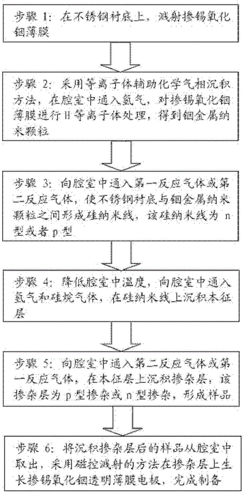
[0020] See figure 1 As shown, the present invention provides a method for preparing a silicon thin film solar cell with a silicon nanowire structure, which includes the following steps:

[0021] Step 1: Sputter a tin-doped indium oxide film on a stainless steel substrate. The mass ratio of tin-steel in the sputtering target is: Sn:In=(0-1):9. Sputtering thickness is 5-10 nanometers;

[0022] Step 2: Using a plasma-assisted chemical vapor deposition method, hydrogen gas is introduced into the chamber, and the tin-doped indium oxide film is subjected to H plasma treatment to obtain indium metal nanoparticles. The power density in the chamber is 0.1W / cm 2 -1.0W / cm 2 , The reaction time is 5 minutes-10 minutes, the reaction gas pressure is 100Pa-200Pa, the chamber temperature is 300℃-450℃, and the diameter of the obtained indium metal nanoparticles is 10-300nm;

[0023] Step 3: Then pass the first reaction gas into the chamber to form silicon nanowires between the stainless steel subst...

Embodiment 2

[0028] It is basically the same as embodiment 1, except that step 3 uses a second reaction gas. The volume ratio of the second reaction gas in the chamber of step 3 is hydrogen, silane gas and borane gas: hydrogen: silane gas :Pure borane gas=100:(1-3):(0.02-0.1), the obtained p-type silicon nanowire

[0029] Step 5 is to use the first reaction gas. In step 5, the first reaction gas in the chamber is hydrogen, silane gas and phosphane gas, and the volume ratio is: hydrogen: silane gas: phosphane gas = 60: (5-10 ): (0.05-0.1), n-type doped, n-type layer obtained.

[0030] See figure 2 , Which is a schematic diagram of the structure of the solar cell obtained by this method, where 1 is a stainless steel substrate, 2 is an n(p) silicon nanowire, 3 is an intrinsic layer silicon film, and 4 is a p(n) layer silicon Thin film, 5 is indium metal nanoparticles, 6 is a transparent conductive film.

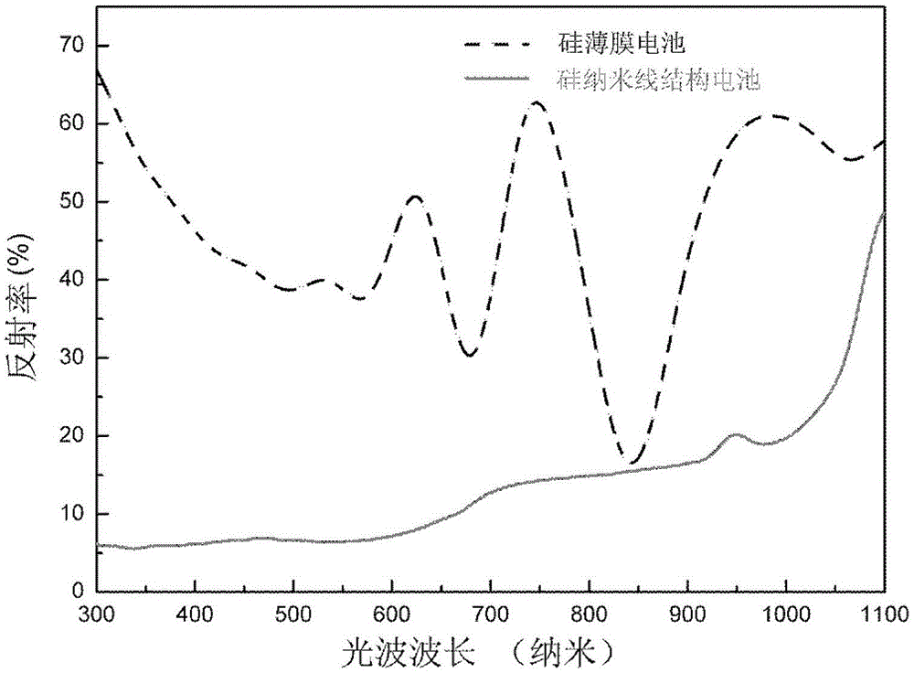
[0031] image 3 The given optical reflection spectrum curve shows that the silicon thin film...


PUM

PropertyMeasurementUnit
Thicknessaaaaaaaaaa
Diameteraaaaaaaaaa
Lengthaaaaaaaaaa

Abstract

Disclosed is a method for preparing silicon thin-film solar cells with silicon nano-wire structures. The method comprises sputtering tin-doped indium oxide film on a stainless steel substrate; feeding hydrogen in a chamber, and performing hydrogen (H) plasma processing on the tin-doped indium oxide film; feeding first reactant gas or second reactant gas in the chamber to enable n-shaped or p-shaped silicon nano-wires to be formed between the stainless steel substrate and indium metal nano-particles; reducing the temperature in the chamber, feeding the hydrogen and silane gas in the chamber, and depositing an intrinsic layer on the silicon nano-wires; feeding the second reactant gas or the first reactant gas in the chamber, and depositing a doping layer on the intrinsic layer to form samples, wherein the doping layer is p-shaped doping or n-shaped doping; and withdrawing the samples with the doping layer deposited from the chamber, and growing tin-doped indium oxide transparent film electrodes on the doping layer through a magnetron sputtering method to complete preparation. The method has high light trapping capacity and photoelectric converting efficiency.

Description

Technical field [0001] The invention belongs to the technical field of solar cells, and particularly relates to a method for preparing a silicon thin film solar cell with a silicon nanowire structure. Background technique [0002] With the depletion of traditional energy sources and the gradual deterioration of the ecological environment, green renewable energy will be the key to solving the energy and environmental crisis. As one of the most abundant clean energy resources on the earth, solar energy has become the first choice for human use. Therefore, how to obtain low-cost and high-efficiency solar cells has attracted the attention of researchers in the world. [0003] Solar cells are devices that directly convert light energy into electrical energy through the photovoltaic effect of semiconductor p-n junctions. At present, the industrialized solar cells are mainly crystalline silicon and various thin film batteries. Crystalline silicon solar cells mainly include monocrystalli...

Claims


Application Information

Patent Timeline
IPC IPC(8): H01L31/18B82Y40/00
CPCY02P70/50
Inventor 谢小兵曾湘波杨萍李洁李敬彦张晓东王启明
Owner INST OF SEMICONDUCTORS - CHINESE ACAD OF SCI
Why Eureka
Try Eureka