A kind of preparation method of p-type gan and algan semiconductor material

A semiconductor, p-type technology, used in semiconductor/solid-state device manufacturing, electrical components, circuits, etc., can solve problems affecting the performance of optoelectronic devices, adverse production and commercial applications, narrow growth windows, etc., to reduce defect density, The effect of improving crystal quality and promoting two-dimensional growth

Active Publication Date: 2018-02-06
SUN YAT SEN UNIV
View PDF6 Cites 0 Cited by
  • Summary
  • Abstract
  • Description
  • Claims
  • Application Information

AI Technical Summary

Problems solved by technology

Although this method can make good use of the hole gas formed by the energy band oscillation of the heterointerface to obtain a higher hole concentration, the superlattice structure is composed of two semiconductor materials with different band gaps alternately stacked and grown. Yes, these two different materials will be different in light absorption intensity and cut-off wavelength, which will affect the performance of optoelectronic devices made using them; acceptor-donor co-doping method (High Doped p-Type GaN Grown by Alternative Co-Doping Technique, Mat.Res. Soc. Symp. Proc. Vol. 719, 2002), although the acceptor-donor Coulomb interaction can be used to effectively reduce the acceptor-doped magnesium atom Ionization energy, but the growth window of this method is very narrow, it is difficult to realize, and it is not conducive to large-scale production and commercial application

Method used


Image

  • A kind of preparation method of p-type gan and algan semiconductor material
  • A kind of preparation method of p-type gan and algan semiconductor material
  • A kind of preparation method of p-type gan and algan semiconductor material

Examples


Embodiment 1

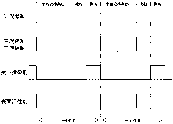
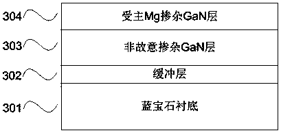
[0037] This implementation case will specifically illustrate figure 1 The growth structure of the p-type GaN semiconductor material shown, as image 3 shown. A buffer layer 302 , an unintentionally doped GaN layer 303 and an acceptor Mg-doped GaN layer 304 are sequentially grown on a sapphire substrate 301 by using a metal organic chemical vapor deposition (MOCVD) epitaxial growth method.

[0038] In the growth process of this embodiment, ammonia gas is used as the source of group V nitrogen; trimethylgallium is used as the source of group III gallium; and trimethylindium is used as a surfactant in the acceptor Mg-doped GaN layer 304 . The implementation of this structure specifically includes the following six steps:

[0039] (1) Place the c-plane sapphire substrate 301 in the reaction chamber, and grow on the sapphire substrate 301 by metal-organic chemical vapor deposition (MOCVD) epitaxial growth method image 3 The epitaxial structure shown.

[0040] (2) The buffer la...

Embodiment 2

[0050] This implementation case will specifically illustrate figure 1 The growth structure of the p-type AlGaN semiconductor material shown, as Figure 5 shown. A buffer layer 502 , an unintentionally doped AlGaN layer 503 and an acceptor Mg-doped AlGaN layer 504 are sequentially grown on a sapphire substrate 501 by a metal organic chemical vapor deposition (MOCVD) epitaxial growth method.

[0051] In the growth process of this implementation case, ammonia gas is used as the source of group V nitrogen; trimethylgallium is used as the source of group III gallium, and trimethylaluminum is used as the source of group III aluminum; trimethylindium is used as a surfactant. The acceptor Mg doped AlGaN layer 304 is used. The implementation of this structure specifically includes the following six steps:

[0052] (1) Place the c-plane sapphire substrate 501 in the reaction chamber, and grow on the sapphire substrate 501 by metal-organic chemical vapor deposition (MOCVD) epitaxial g...


PUM

PropertyMeasurementUnit
thicknessaaaaaaaaaa
thicknessaaaaaaaaaa
thicknessaaaaaaaaaa

Abstract

The invention discloses a method for preparing p-type GaN and AlGaN semiconductor materials, including a substrate, a buffer layer or transition layer grown on the substrate from bottom to top, an unintentional doped layer and an acceptor doped layer; During the growth of the structure, use ammonia or dimethylhydrazine nitrogen as the source of group V nitrogen; use trimethylgallium or triethylgallium as the source of group III gallium, and use trimethylaluminum or triethylaluminum as the source of group III aluminum Source, using trimethylindium or triethylindium as the source of group III indium, collectively referred to as the source of group III metals; trimethylindium or triethylindium is also used as a surfactant in the acceptor doped layer. The present invention uses trimethyl indium or triethyl indium as surfactant to assist growth, and adopts delta doping method to prepare acceptor doping layer. The method increases the doping efficiency of acceptor-doped magnesium atoms, and at the same time suppresses its self-compensation effect, thereby obtaining p-type GaN and AlGaN semiconductor materials with good crystal quality and high hole concentration.

Description

technical field [0001] The invention relates to the technical field of epitaxial growth of p-type GaN and AlGaN semiconductor materials, in particular to a method for preparing p-type GaN and AlGaN semiconductor materials by using surfactant-assisted delta doping. Background technique [0002] Group III nitrides (also known as GaN-based materials), as the third-generation semiconductor materials, have the characteristics of large band gap, direct band gap (high photoelectric conversion efficiency), stable chemical properties, strong thermal conductivity and high breakdown voltage. Based on this type of semiconductor material, optoelectronic devices with high photoelectric conversion efficiency and high response speed (such as blue-green light-emitting diodes, semiconductor lasers and ultraviolet photodetectors) and high-temperature resistant, high-voltage resistant, high-power electronic devices ( Such as high electron mobility transistors and high power switching field effe...

Claims


Application Information

Patent Timeline
Patent Type & Authority Patents(China)
IPC IPC(8): H01L21/205
Inventor 江灏陈英达
Owner SUN YAT SEN UNIV
Why Eureka
Try Eureka