


Quick Research
Generate reliable direction feasibility study reports for your R&D in just a few steps.

Technical Q&A
Discover and master advanced knowledge NOW. Basics, ideas, possibilities, all at once.

Find Solutions
As an expert in R&D theories, this can generate solutions to your technical problems instantly.

Evaluate Feasibility
Analyze your overall solution with one click, know your potential R&D risks in advance.

Monitor Landscape
Get weekly tech updates, stay abreast of the latest tech innovations and key insights.
Fabrication method of CMOS (complementary metal-oxide-semiconductor transistor) transistor
A fabrication method and transistor technology, which are applied in semiconductor/solid-state device manufacturing, electrical components, circuits, etc., can solve problems such as extrusion of semiconductor substrates, deformation of stress layers, and performance degradation of semiconductor devices, and achieve improved performance and yield. Effect
- Summary
- Abstract
- Description
- Claims
- Application Information
AI Technical Summary
Problems solved by technology
Method used
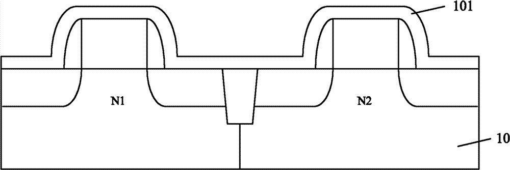
Image


Examples
Embodiment Construction
[0029] In the prior art, in the process of manufacturing CMOS devices, spike annealing is usually used to activate the ions of the source / drain; the tensile stress of the surface stress layer of the NMOS transistor is applied to the bottom channel region by laser annealing to improve the carrier mobility , reduce the threshold voltage, etc. However, if spike annealing is used first, and then laser annealing is used, laser annealing will cause the stress layer to deform, and the semiconductor substrate will be squeezed, resulting in greater damage that cannot be repaired; laser annealing is used first, and then spike annealing is used, When the source / drain is caused, damage and defects generated in the semiconductor substrate are activated, causing an increase in the parasitic resistance between the source / drain.
[0030] In view of the above problems, the inventors of the present invention first performed the first peak annealing process in the process of making CMOS transist...
PUM
| Property | Measurement | Unit |
|---|---|---|
| Wavelength | aaaaa | aaaaa |
Abstract
Description
Claims
Application Information
 - R&D Engineer
- R&D Manager
- IP Professional
- Industry Leading Data Capabilities
- Powerful AI technology
- Patent DNA Extraction
Browse by: Latest US Patents, China's latest patents, Technical Efficacy Thesaurus, Application Domain, Technology Topic, Popular Technical Reports.
© 2024 PatSnap. All rights reserved.Legal|Privacy policy|Modern Slavery Act Transparency Statement|Sitemap|About US| Contact US: help@patsnap.com