Manufacturing method of embedded epitaxial layer

A manufacturing method and epitaxial layer technology, applied in semiconductor/solid-state device manufacturing, electrical components, circuits, etc., can solve the problems of reducing carrier mobility in the channel region, collapse of the silicon-germanium main layer 106b, and reducing device performance, etc. Achieve size reduction, low cost, improve performance and yield

Pending Publication Date: 2021-07-20
SHANGHAI HUALI INTEGRATED CIRCUTE MFG CO LTD
View PDF0 Cites 0 Cited by
  • Summary
  • Abstract
  • Description
  • Claims
  • Application Information

AI Technical Summary

Problems solved by technology

The doping concentration of the silicon-germanium main layer 106b, that is, the concentration of germanium is a fixed value, and defects are easily generated during growth, so that the grown silicon-germanium main layer 106b collapses as shown by the dotted circle 107
The volume of the collapsed silicon germanium main body layer 106b is reduced, and the stress on the silicon substrate 101 on both sides of the groove 105 is also reduced, and finally the carrier mobility in the channel region will be reduced, thereby reducing Device performance

Method used


Image

  • Manufacturing method of embedded epitaxial layer
  • Manufacturing method of embedded epitaxial layer
  • Manufacturing method of embedded epitaxial layer

Examples


Embodiment Construction

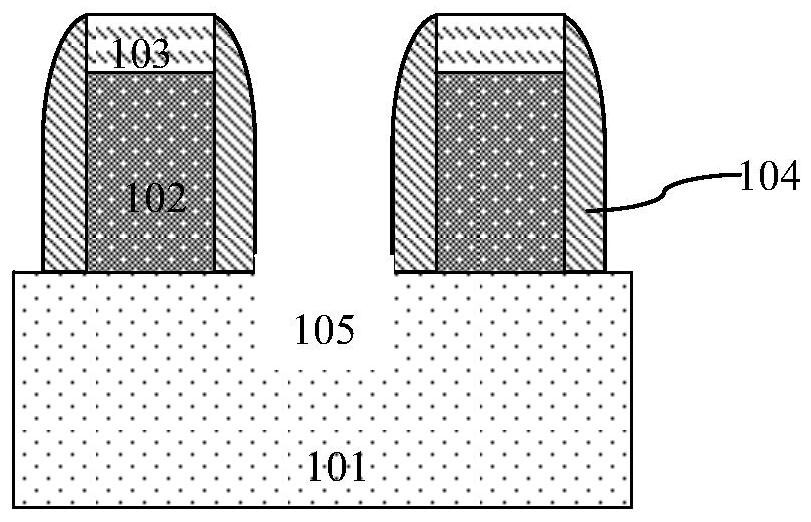
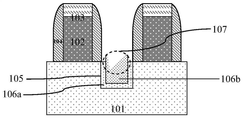
[0064] Such as Figure 4 As shown, it is a flow chart of the manufacturing method of the embedded epitaxial layer 6 according to the embodiment of the present invention; as Figure 5A to Figure 5D As shown, it is a schematic diagram of the device structure in each step of the manufacturing method of the embedded epitaxial layer 6 in the embodiment of the present invention; the manufacturing method of the embedded epitaxial layer 6 in the embodiment of the present invention includes the following steps:

[0065] Step 1, such as Figure 5A As shown, the silicon substrate 1 is etched to form grooves 5 .

[0066] A gate structure is formed on the silicon substrate 1, and the groove 5 is self-aligned and formed on two sides of the gate structure.

[0067] The gate structure includes a gate dielectric layer and a polysilicon gate 2 stacked in sequence.

[0068] The top of the polysilicon gate 2 is covered with a top hard mask layer 3 , and side walls 4 are formed on the side of t...


PUM


Abstract

The invention discloses a manufacturing method of an embedded epitaxial layer. The method comprises the following steps of: step 1, etching a silicon substrate to form a groove; and step 2, filling the groove with an embedded epitaxial layer: step 21, forming a buffer layer; step 22, forming a main body layer on the surface of the buffer layer; doping the main body layer in silicon to provide stress for the silicon substrate at the two sides of the groove, wherein the doping concentration of the main body layer is gradually varied in the epitaxial growth process to eliminate the fault defect and further prevent the main body layer from collapsing; step 23, forming a cap layer, and superposing the buffer layer, the main body layer and the cap layer to form an embedded epitaxial layer; wherein the buffer layer, the main body layer and the cap layer are made of the same material, and the doping concentration of the buffer layer and the cap layer is smaller than or equal to the minimum doping concentration of the main body layer. According to the invention, the main body layer of the embedded epitaxial layer can be prevented from collapsing, so that the performance and the yield of a product can be improved.

Description

technical field [0001] The invention relates to a method for manufacturing a semiconductor integrated circuit, in particular to a method for manufacturing an embedded epitaxial layer. Background technique [0002] With the development of technology, the critical dimension (CD) of the device is getting smaller and smaller. When the process node of the device is below 28nm, it is often necessary to use embedded epitaxial layers in the source and drain regions to change the stress of the channel region, thereby increasing the current carrying capacity. Mobility of electrons and thus improve the performance of the device. For PMOS devices, the embedded epitaxial layer usually adopts silicon germanium epitaxial layer (SiGe); for NMOS devices, the embedded epitaxial layer usually adopts phosphorus silicon epitaxial layer (SiP). [0003] Usually, after the gate structure of the device is formed, grooves are formed by self-alignment on both sides of the gate structure; then, an emb...

Claims


Application Information

Patent Timeline
IPC IPC(8): H01L21/336H01L29/78H01L29/08H01L29/36
CPCH01L29/66477H01L29/66795H01L29/7848H01L29/785H01L29/0847H01L29/36
Inventor 涂火金张瑜
Owner SHANGHAI HUALI INTEGRATED CIRCUTE MFG CO LTD
Why Eureka
Try Eureka