


Quick Research
Generate reliable direction feasibility study reports for your R&D in just a few steps.

Technical Q&A
Discover and master advanced knowledge NOW. Basics, ideas, possibilities, all at once.

Find Solutions
As an expert in R&D theories, this can generate solutions to your technical problems instantly.

Evaluate Feasibility
Analyze your overall solution with one click, know your potential R&D risks in advance.

Monitor Landscape
Get weekly tech updates, stay abreast of the latest tech innovations and key insights.
Wafer and manufacturing method thereof, and electronic device
A manufacturing method and wafer technology, applied in semiconductor/solid-state device manufacturing, circuits, electrical components, etc., can solve problems such as wafer particle pollution, restriction of wafer performance and yield, wafer fragmentation, etc., to improve performance and yield rate effect
- Summary
- Abstract
- Description
- Claims
- Application Information
AI Technical Summary
Problems solved by technology
Method used
Image

Examples
Embodiment 1
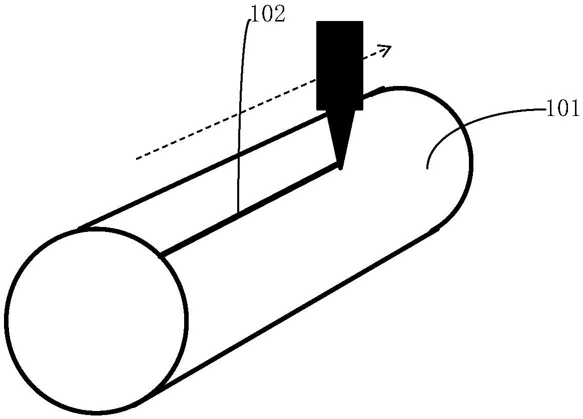
[0047] In order to solve the aforementioned technical problems and improve the performance of the device, an embodiment of the present invention provides a method for manufacturing a semiconductor device, such as figure 2 Said, said method mainly comprises:
[0048] Step S1: providing a silicon ingot;
[0049] Step S2: forming a linear film mark for marking the crystal direction of the silicon ingot on the side of the silicon ingot;
[0050] Step S3: slicing the silicon ingot to form a silicon wafer;
[0051] Step S4: Forming a laser mark for marking the crystal direction of the silicon ingot on any one of the upper and lower bottom surfaces of the silicon wafer with the linear film layer mark as a reference;
[0052] Step S5: removing the linear film layer mark.
[0053] According to the wafer manufacturing method of the present invention, in order to mark the crystal orientation of the wafer, a removable linear film layer mark is first formed, and a laser mark is formed ...
Embodiment 2
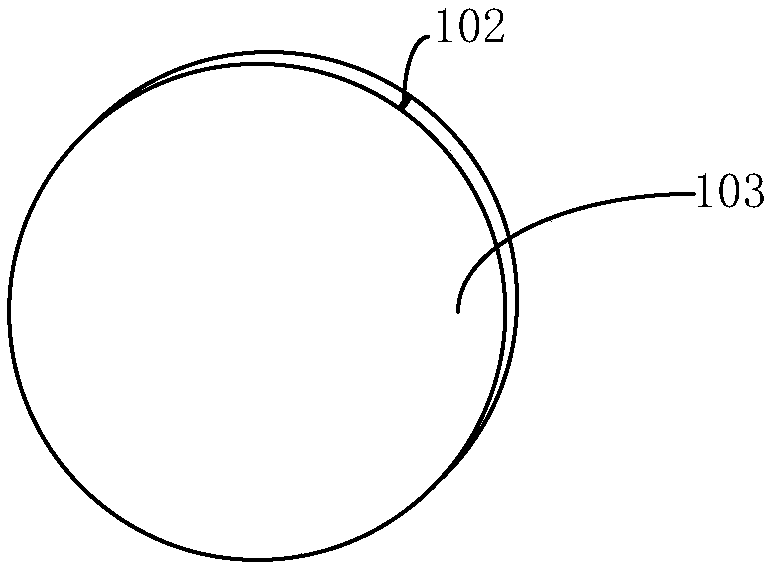
[0100] The present invention also provides a wafer, which is prepared by the method described in the first embodiment.
[0101] Wherein, a laser mark is formed on the wafer instead of a wafer notch or a wafer face-taking mark.
[0102] Wherein, the wafer is silicon polycrystalline or silicon single crystal, and is not limited to a certain one.
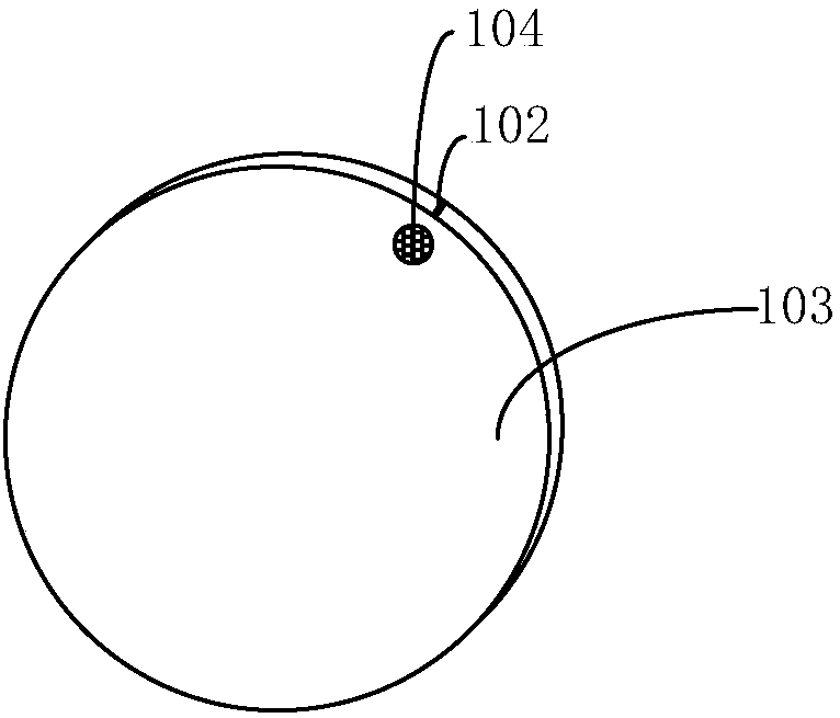
[0103] Wherein, the laser mark 104 is formed in a predetermined area by means of laser radiation.
[0104] Wherein, in this step, a pulsed laser with a frequency of 10 MHz or higher may be used to act on the surface of the wafer to form the laser mark 104 .
[0105] Wherein, the shape of the laser mark 104 may be a circle, a square, a polygon, etc., and is not limited to a certain one.
[0106] In this embodiment, the laser mark 104 is circular with a diameter of 0.5-5mm, but it is not limited to this range.
[0107] There is no etching step in the preparation process of the wafer and the laser mark, which can avoid the chipping of ...
Embodiment 3
[0109] Another embodiment of the present invention provides an electronic device, which includes a wafer, the wafer is the wafer in the second embodiment above, or a wafer prepared according to the wafer preparation method described in the first embodiment .
[0110] The electronic device can be any electronic product or equipment such as mobile phone, tablet computer, notebook computer, netbook, game console, TV, VCD, DVD, navigator, camera, video camera, recording pen, MP3, MP4, PSP, etc. It is an intermediate product with the above-mentioned semiconductor, for example: a mobile phone motherboard with the integrated circuit, etc.
[0111] in, image 3 An example of a mobile phone handset is shown. The mobile phone handset 300 is provided with a display portion 302 included in a housing 301, operation buttons 303, an external connection port 304, a speaker 305, a microphone 306, and the like.
[0112] Wherein said mobile phone handset comprises the aforementioned wafer,
...
PUM
| Property | Measurement | Unit |
|---|---|---|
| Diameter | aaaaa | aaaaa |
| Thickness | aaaaa | aaaaa |
Abstract
Description
Claims
Application Information
 - R&D Engineer
- R&D Manager
- IP Professional
- Industry Leading Data Capabilities
- Powerful AI technology
- Patent DNA Extraction
Browse by: Latest US Patents, China's latest patents, Technical Efficacy Thesaurus, Application Domain, Technology Topic, Popular Technical Reports.
© 2024 PatSnap. All rights reserved.Legal|Privacy policy|Modern Slavery Act Transparency Statement|Sitemap|About US| Contact US: help@patsnap.com