Six-transistor static random access memory unit and manufacturing method thereof

A memory unit, static random technology, applied in static memory, semiconductor/solid-state device manufacturing, transistors, etc., can solve the problems of shortened device life, low degree of asymmetry, unstable reading and writing, etc., to achieve simple process and reduce cost Effect

Active Publication Date: 2012-11-14
SHANGHAI INST OF MICROSYSTEM & INFORMATION TECH CHINESE ACAD OF SCI
View PDF3 Cites 10 Cited by
  • Summary
  • Abstract
  • Description
  • Claims
  • Application Information

AI Technical Summary

Problems solved by technology

[0005] In view of the above-mentioned shortcomings of the prior art, the object of the present invention is to provide a six-transistor SRAM unit and a manufacturing method thereof, which are used to solve the problem of reading and writing caused by the low asymmetry of the six-transistor SRAM unit in the prior art. Instability, or the problem of shortening the life of the device in order to increase the degree of asymmetry of the device

Method used


Image

  • Six-transistor static random access memory unit and manufacturing method thereof
  • Six-transistor static random access memory unit and manufacturing method thereof
  • Six-transistor static random access memory unit and manufacturing method thereof

Examples


Embodiment 1

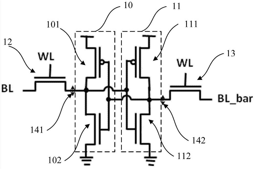
[0055] Such as Figure 1~Figure 3 As shown, the present invention provides a six-transistor SRAM unit, the memory unit at least includes:

[0056] The first inverter 10 is composed of a first PMOS transistor 101 and a first NMOS transistor 102;

[0057] The second inverter 11 is composed of a second PMOS transistor 111 and a second NMOS transistor 112;

[0058] The transmission gate is composed of a third NMOS transistor 12 and a fourth NMOS transistor 13;

[0059] Wherein, the source of the third NMOS transistor 12 is connected to the output terminal of the first inverter 10 and the input terminal of the second inverter 11 at the same time, the gate is connected to the word line of the memory, and the drain is connected to the memory the bit line;

[0060] The source of the fourth NMOS transistor 13 is connected to the input terminal of the first inverter 10 and the output terminal of the second inverter 11 at the same time, the gate is connected to the word line of the me...

Embodiment 2

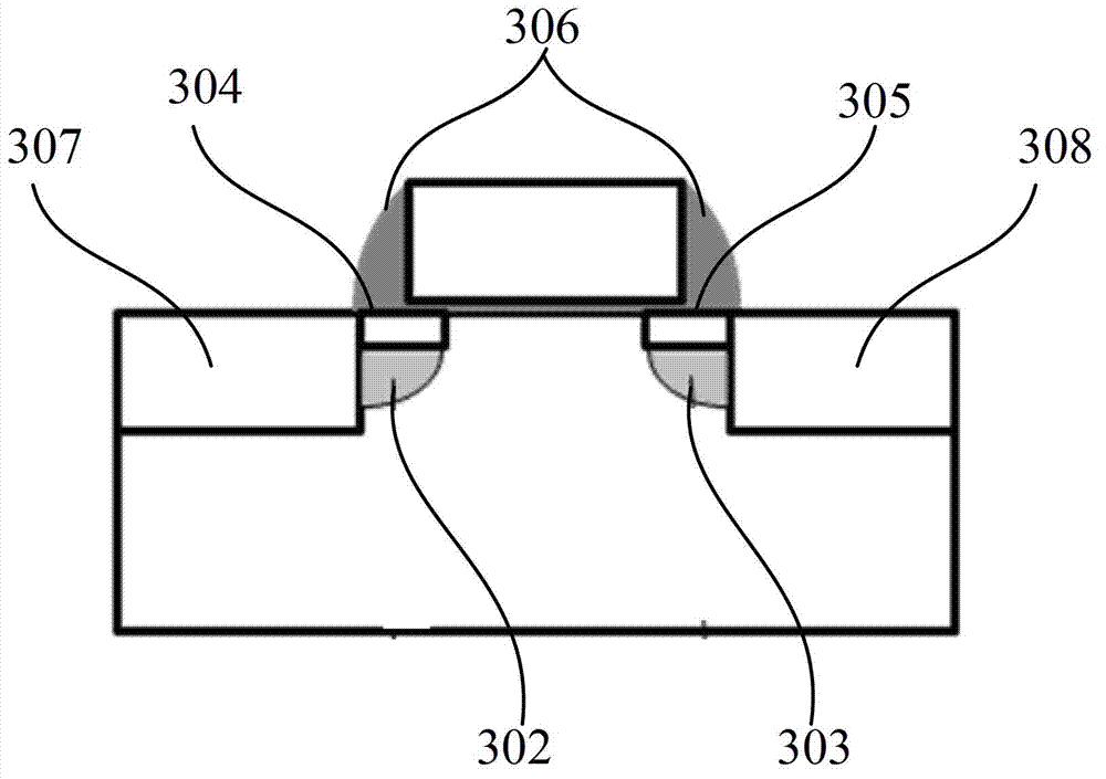
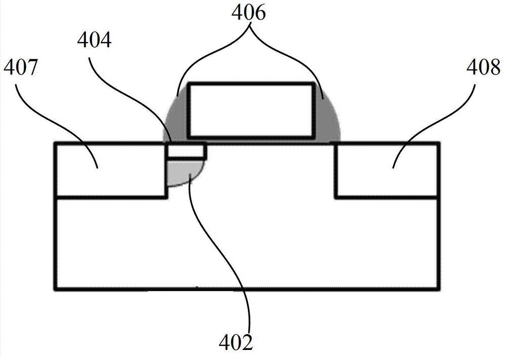
[0068] see Figure 2~3 and Figure 4~7 This embodiment provides a method for manufacturing a six-transistor SRAM unit, and the method at least includes the following steps:

[0069] Such as Figure 4 As shown, step 1) is first performed, providing a semiconductor substrate, and defining active regions 20a, 20b, 20c and 20d in the semiconductor substrate, and forming shallow trench isolation trenches around the active region ( not shown); specifically, the active regions 20a, 20b, 20c and 20d are defined first, then shallow trenches are etched around the active regions, and finally insulating materials are filled in the shallow trenches to form the Shallow trench isolation trenches. In this embodiment, the semiconductor substrate is a bulk silicon substrate or a silicon-on-insulator substrate, and the insulating material is silicon dioxide.

[0070] Such as Figure 5 shown, and then proceed to step 2) to form an N-type well implantation region 22 in the semiconductor subst...


PUM


Abstract

The invention provides a six-transistor static random access memory unit and a manufacturing method thereof, and belongs to the technical field of memory design and manufacturing. The memory unit comprises two phase inverters and a transmission gate, wherein each phase inverter consists of an N-channel metal oxide semiconductor (NMOS) transistor with a symmetric structure and a P-channel metal oxide semiconductor (PMOS) with a symmetric structure, and the NMOS transistor and the PMOS transistor are connected with each other; the transmission gate consists of two NMOS transistors with asymmetric source and drain structures; and the source structure of each NMOS transistor with the asymmetric source and drain structure is provided with a pocket domain and a lightly doped domain, and the drain structure is not provided with the pocket domain and the lightly doped domain. According to the six-transistor static random access memory unit, the transmission gate N-type transistors with the asymmetric structures are adopted; the processing technique of the device is not changed, extra domains are not increased, the service life of the device is not shortened, and the electrical asymmetry is obviously higher than that of the conventional structure by removing the asymmetry caused by the lightly doped domain (LDD) and the pocket domain of the drain. The invention is simple in technique, is beneficial to cost reduction, and is suitable for industrial production.

Description

technical field [0001] The invention belongs to the technical field of memory design and manufacture, and in particular relates to a six-transistor static random access memory unit and a manufacturing method thereof. Background technique [0002] The memory is divided into flash memory (Flash), dynamic random access memory (DRAM) and static random access memory (SRAM). Among them, static random access memory has become the first choice for key system storage modules because of its fast read and write and no need for periodic refresh, such as CPU and Cache between main memory, etc. Although the static memory occupies a larger area than other memories at the same storage capacity, it still cannot be replaced by other new types of memories in the case of fast read and write. [0003] Currently commonly used SRAM cells mainly use six transistors, which are composed of two pull-up P-type transistors, two pull-down N-type transistors and two transfer-gate N-type transistors. The...

Claims


Application Information

Patent Timeline
Patent Type & Authority Applications(China)
IPC IPC(8): H01L29/08H01L27/11H01L21/8244G11C11/413H10B10/00
CPCH01L29/66659H01L27/1104G11C11/412H01L29/7835H10B10/12
Inventor 陈静伍青青罗杰馨柴展余涛王曦
Owner SHANGHAI INST OF MICROSYSTEM & INFORMATION TECH CHINESE ACAD OF SCI
Why Eureka
Try Eureka