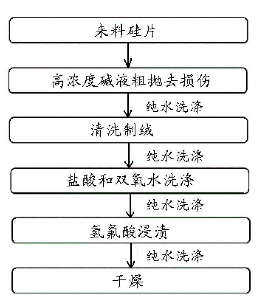
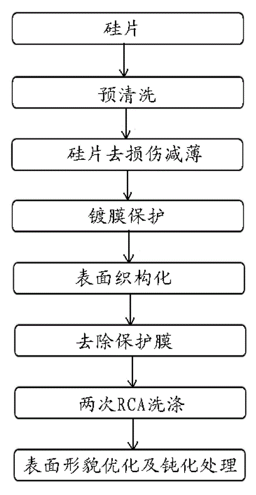
Wet surface processing technique used for manufacturing high efficiency crystalline silicon solar cells
A crystalline silicon solar cell, wet processing technology, applied in the direction of post-processing, post-processing details, sustainable manufacturing/processing, etc., can solve the problems of increasing battery cost, difficult fragmentation rate, etc., to reduce process cost and improve quality. Effect
- Summary
- Abstract
- Description
- Claims
- Application Information
AI Technical Summary
Problems solved by technology
Method used
Image
Examples
specific Embodiment 1
[0037] A surface wet treatment process for making high-efficiency crystalline silicon solar cells has the following steps:
[0038] (1) Pre-cleaning: Place the silicon wafer in absolute ethanol for ultrasonic cleaning, and then treat it with RCA solution and hydrofluoric acid to remove inorganic metal ions and organic particle pollutants.
[0039] The silicon wafer is placed in absolute ethanol for 10 minutes for ultrasonic cleaning, and the RCA solution has a volume ratio of DI:NH 4 OH:H 2 o 2 =4:1:1 solution, the RCA solution treatment temperature is 65-85°C, the treatment time is 5-20min, the hydrofluoric acid concentration is 5wt%, and the hydrofluoric acid immersion time is 2min.
[0040] After the above treatment, the inorganic metal ions and organic particle pollutants on the surface of the silicon wafer can be effectively removed.
[0041] (2) Damage and thinning of the silicon wafer: the mechanically damaged layer on the surface of the silicon wafer and the residua...
specific Embodiment 2
[0052] A surface wet treatment process for making high-efficiency crystalline silicon solar cells has the following steps:
[0053] (1) Pre-cleaning: Place the silicon wafer in absolute ethanol for ultrasonic cleaning, and then treat it with RCA solution and hydrofluoric acid to remove inorganic metal ions and organic particle pollutants.
[0054] The silicon wafer is placed in absolute ethanol for 10 minutes for ultrasonic cleaning, and the RCA solution has a volume ratio of DI:NH 4 OH:H 2 o 2 =4:1:1 solution, the RCA solution treatment temperature is 65-85°C, the treatment time is 5-20min, the hydrofluoric acid concentration is 5wt%, and the hydrofluoric acid immersion time is 2min.
[0055] After the above treatment, the inorganic metal ions and organic particle pollutants on the surface of the silicon wafer can be effectively removed.
[0056] (2) Damage and thinning of the silicon wafer: the mechanically damaged layer on the surface of the silicon wafer and the residua...
specific Embodiment 3
[0067] A surface wet treatment process for making high-efficiency crystalline silicon solar cells has the following steps:
[0068] (1) Pre-cleaning: Place the silicon wafer in absolute ethanol for ultrasonic cleaning, and then treat it with RCA solution and hydrofluoric acid to remove inorganic metal ions and organic particle pollutants.
[0069] The silicon wafer is placed in absolute ethanol for 10 minutes for ultrasonic cleaning, and the RCA solution has a volume ratio of DI:NH 4 OH:H 2 o 2 =4:1:1 solution, the RCA solution treatment temperature is 65-85°C, the treatment time is 5-20min, the hydrofluoric acid concentration is 2.5wt%, and the hydrofluoric acid immersion time is 2min.
[0070] After the above treatment, the inorganic metal ions and organic particle pollutants on the surface of the silicon wafer can be effectively removed.
[0071] (2) Damage and thinning of the silicon wafer: the mechanically damaged layer on the surface of the silicon wafer and the resid...
PUM
 Abstract
Description
Claims
Application Information
 - R&D
- Intellectual Property
- Life Sciences
- Materials
- Tech Scout
- Unparalleled Data Quality
- Higher Quality Content
- 60% Fewer Hallucinations
Browse by: Latest US Patents, China's latest patents, Technical Efficacy Thesaurus, Application Domain, Technology Topic, Popular Technical Reports.
© 2025 PatSnap. All rights reserved.Legal|Privacy policy|Modern Slavery Act Transparency Statement|Sitemap|About US| Contact US: help@patsnap.com


