Super junction device terminal protection structure and manufacturing method thereof

A terminal protection structure and super junction technology, which is applied in semiconductor/solid-state device manufacturing, electric solid-state devices, semiconductor devices, etc., can solve different problems

Active Publication Date: 2012-10-17
SHANGHAI HUAHONG GRACE SEMICON MFG CORP
View PDF5 Cites 4 Cited by
  • Summary
  • Abstract
  • Description
  • Claims
  • Application Information

AI Technical Summary

Problems solved by technology

[0003] For existing devices such as high-voltage VDMOS, there are diffusion guard ring technologies and field plate technologies such as floating field plate technology, resistive field plate technology, equipotential ring technology, field limiting ring technology, ju...

Method used


Image

  • Super junction device terminal protection structure and manufacturing method thereof
  • Super junction device terminal protection structure and manufacturing method thereof
  • Super junction device terminal protection structure and manufacturing method thereof

Examples


Embodiment Construction

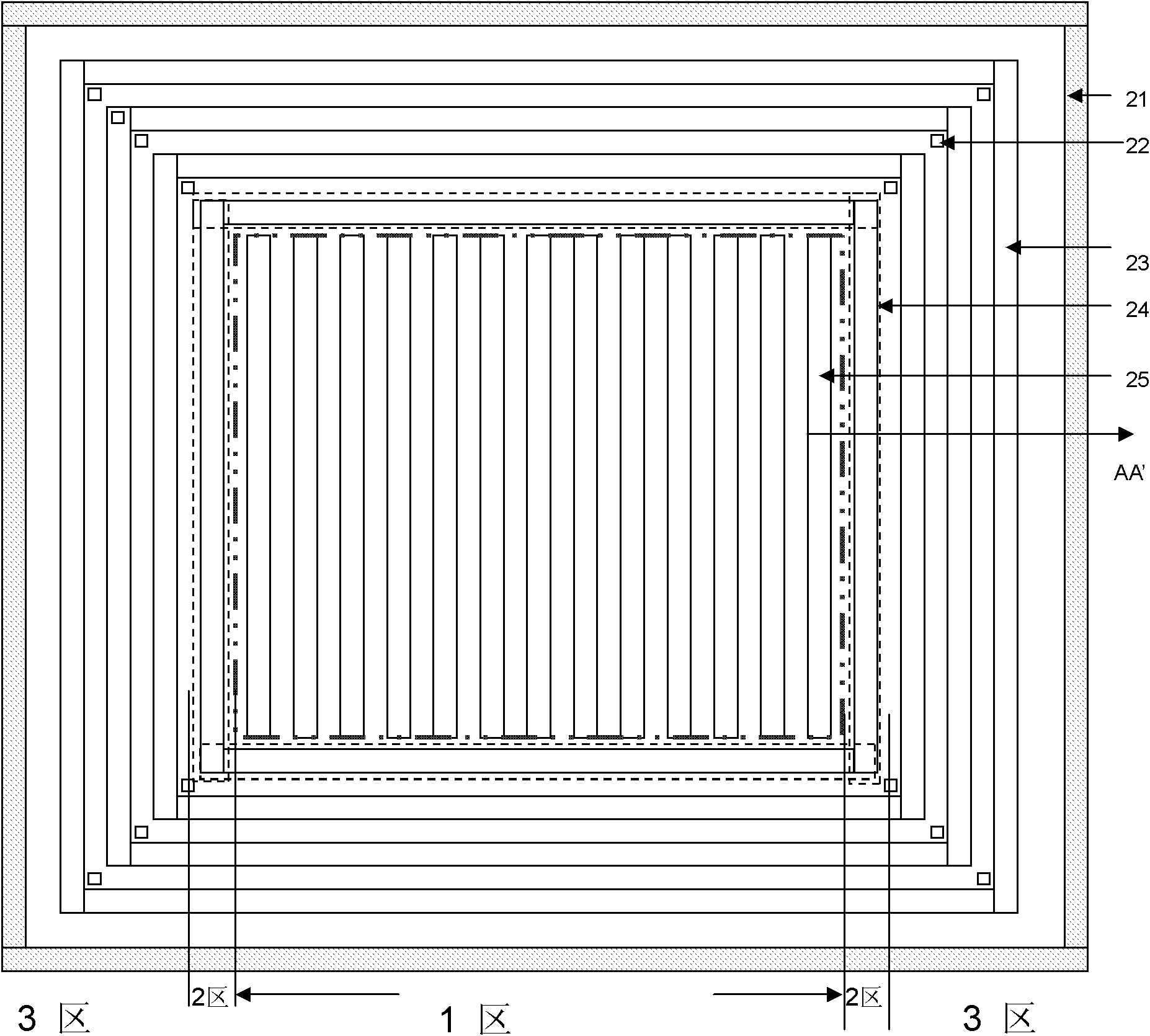
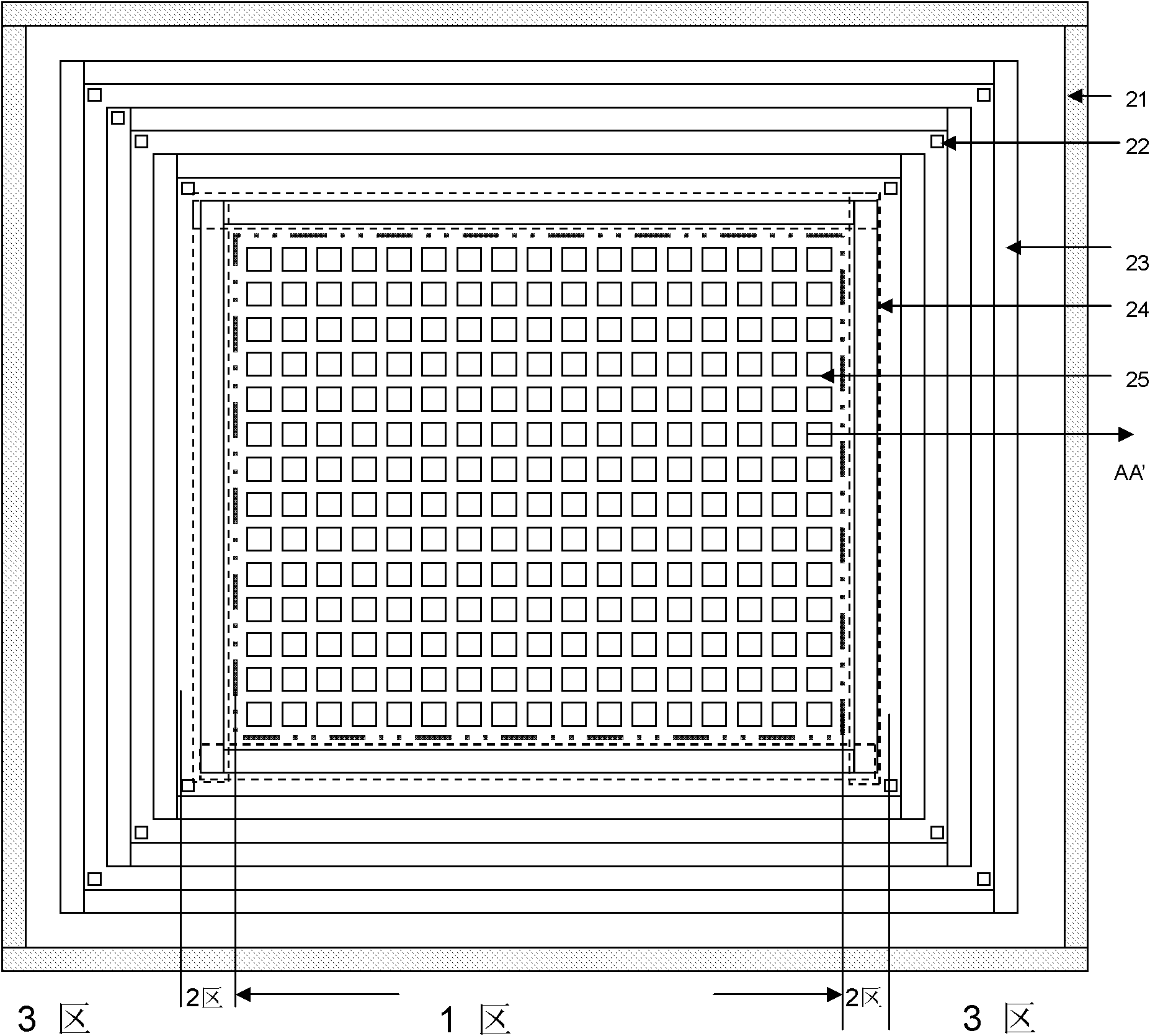
[0122] Such as figure 1 As shown, it is a top view of the terminal protection structure of the super junction device according to the embodiment of the present invention Figure 1 . In the top view, the embodiment of the present invention can be divided into zone 1, zone 2 and zone 3. Region 1 is the middle region of the super junction device, which is the current flow region, and the current flow region includes alternately arranged P-type regions 25 and N-type regions formed in the N-type epitaxial layer; in the current flow region, the current flows Through the N-type region, the source passes through the channel to reach the drain, and the P-type region 25 bears voltage together with the depletion region formed by the N-type region in the reverse cut-off state. Regions 2 and 3 are the terminal protection structure regions of the super junction device. The terminal protection structure does not provide current when the device is turned on, and is used to bear the peripher...


PUM

PropertyMeasurementUnit
Tilt angleaaaaaaaaaa

Abstract

The invention discloses a terminal protection structure of a super junction device. The composite structure of polysilicon field plates and metal field plates is employed, and a group of polysilicon field plates and metal field plates simultaneously cover the step structure of a terminal dielectric film, thus an electric field on the device surface is eased. According to the invention, a P-type ring with a high concentration is kept under a field plate, thus the current processing capability of the application of the device in an inductive circuit is improved. In the terminal protection structure provided by the invention, the depth of a P-type column and a N-type column is lower than the depth of a P-type area and a N-type area in a current flowing area to ensure that the device is turned off when the device is applied in the inductive circuit and that the position where an avalanche breakdown occurs in the terminal protection structure is close to the position of the obverse of a silicon chip when a current overshoot occurs, and to improve the capacity of anti-overshoot current of the device. The invention further discloses the super junction device terminal protection structure and a manufacturing method thereof. According to the invention, the breakdown characteristic, the current processing capability and the reliability of the device is improved without process cost increasement.

Description

technical field [0001] The invention relates to the field of semiconductor integrated circuit manufacturing, in particular to a terminal protection structure of a super junction device; the invention also relates to a manufacturing method of the terminal protection structure of a super junction device. Background technique [0002] The super junction MOSFET adopts a new voltage-resistant layer structure, and uses a series of alternately arranged P-type semiconductor thin layers and N-type semiconductor thin layers to combine the P-type semiconductor thin layers and N-type semiconductor thin layers at a lower voltage in the off state. The thin layer of semiconductor is depleted to achieve mutual compensation of charges, so that the thin layer of P-type semiconductor and thin layer of N-type semiconductor can achieve high breakdown voltage under high doping concentration, so as to obtain low on-resistance and high breakdown at the same time voltage, breaking the theoretical li...

Claims


Application Information

Patent Timeline
IPC IPC(8): H01L29/06H01L27/02H01L21/336
Inventor 肖胜安
Owner SHANGHAI HUAHONG GRACE SEMICON MFG CORP
Why Eureka
Try Eureka