Method for preparing organic field effect transistor structure
A transistor and organic field technology, applied in the field of organic electronics, can solve the problems of complex process and mutual interference of modifiers, and achieve the effect of improving growth quality, mobility and injection efficiency
- Summary
- Abstract
- Description
- Claims
- Application Information
AI Technical Summary
Problems solved by technology
Method used
Image


Examples
preparation example Construction
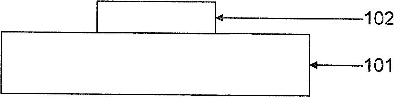
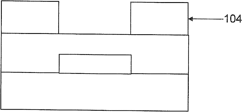
[0032] Figure 1-1 to Figure 1-5 The flow chart of the method for preparing the organic field effect transistor structure provided by the present invention mainly includes the following steps:
[0033] like Picture 1-1 As shown, the patterned gate electrode 102 is prepared on the insulating substrate 101, and the thin film deposition method of the gate electrode layer includes vacuum thermal physical deposition, electron beam deposition, ion-assisted deposition, sputtering, ink jet printing, and spin coating. The insulating substrate 101 is the supporting part of the electrode, the gate dielectric and the organic semiconductor thin film layer, and the substrate should have a relatively low surface roughness and a certain ability of water vapor and oxygen permeation. Including silicon wafers with insulating films such as silicon oxide and silicon nitride, insulating glass and insulating plastic films. Materials of the gate electrode 102 thin film include gold, aluminum, plati...
Embodiment 1
[0039] The specific preparation method of the organic field effect transistor provided by this embodiment is as follows:
[0040] Step 1: On the silicon wafer substrate with 300nm silicon oxide, the photoresist pattern of the gate electrode is first prepared by photolithography process, and then a layer of 100nm thick aluminum metal film is deposited by electron beam evaporation. Photoresist and metal films are required to form patterned aluminum metal gate electrodes.
[0041] In step 2, an aluminum oxide film with a thickness of 30 nm is prepared on the aluminum metal gate electrode by atomic layer deposition technology as a gate dielectric.
[0042] Step 3: On the surface of the first type of gate dielectric layer, the photoresist pattern of the source and drain electrodes is first prepared by a photolithography process, and then a 50nm thick gold metal film is deposited by electron beam evaporation, and the unwanted light is removed by a lift-off process. Resist and metal...
Embodiment 2
[0046] The specific preparation method of the organic field effect transistor provided by this embodiment is as follows:
[0047] Step 1, on a flexible polyethylene naphthalate (PEN) film substrate, a photoresist pattern of the gate electrode is first prepared by a photolithography process, and then a layer of 100 nm thick aluminum metal film is deposited by electron beam evaporation, Unwanted photoresist and metal film are removed by a metal lift-off process to form a patterned aluminum metal gate electrode.
[0048] In step 2, an aluminum oxide film with a thickness of 30 nm is prepared on the aluminum metal gate electrode by atomic layer deposition technology as a gate dielectric.
[0049] Step 3: On the surface of the first type of gate dielectric layer, the photoresist pattern of the source and drain electrodes is first prepared by a photolithography process, and then a 50nm thick gold metal film is deposited by electron beam evaporation, and the unwanted light is removed...
PUM
 Abstract
Description
Claims
Application Information
 - R&D
- Intellectual Property
- Life Sciences
- Materials
- Tech Scout
- Unparalleled Data Quality
- Higher Quality Content
- 60% Fewer Hallucinations
Browse by: Latest US Patents, China's latest patents, Technical Efficacy Thesaurus, Application Domain, Technology Topic, Popular Technical Reports.
© 2025 PatSnap. All rights reserved.Legal|Privacy policy|Modern Slavery Act Transparency Statement|Sitemap|About US| Contact US: help@patsnap.com