Method for forming nanometer gradient structure on surface layer of shaft metallic material
A technology of metal material and gradient structure, which is applied in the field of processing where plastic deformation occurs on the surface of the material, can solve the problems of large surface roughness, poor surface finish, and difficulty in forming nano-crystal structures on the surface of the workpiece, and achieve low surface roughness, The processing method is simple and the force is uniform
- Summary
- Abstract
- Description
- Claims
- Application Information
AI Technical Summary
Problems solved by technology
Method used
Image
Examples
Embodiment 1
[0034] Utilize processing method of the present invention to process 316L stainless steel:
[0035] Equipment: CNC lathe;
[0036] 316L stainless steel diameter: 12mm in diameter;
[0037] Spindle (processed workpiece) speed: line speed 300 mm / s;
[0038] Each feeding amount: 30 microns / time;
[0039] Axial feed speed: 20mm / min;
[0040] Ball diameter: 8 mm;
[0041]Deformation temperature: room temperature;
[0042] Processing times: 6 times;
[0043] The grain size of 316L stainless steel before processing is 2-3 microns.
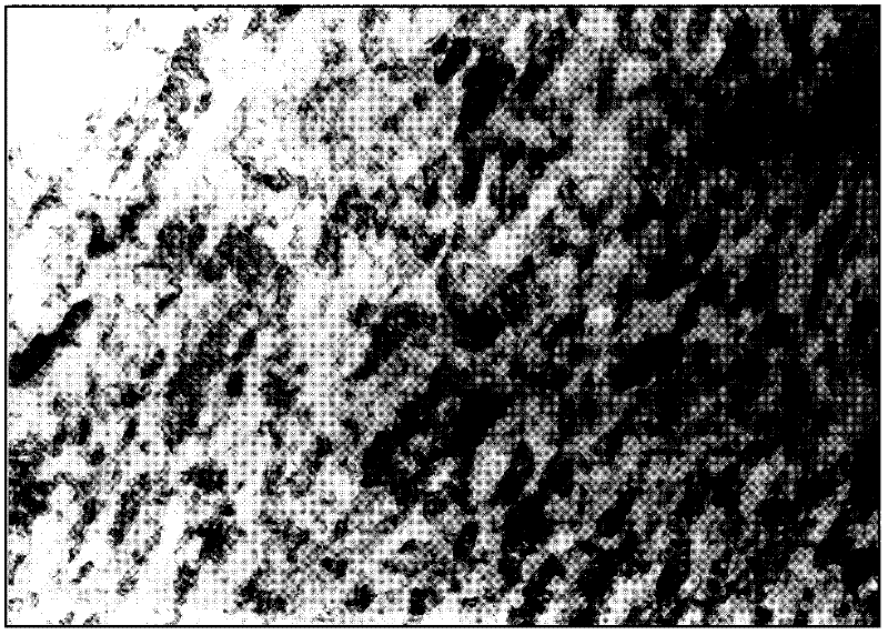
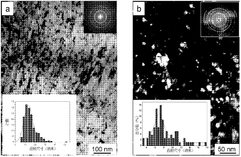
[0044] 316L stainless steel after treatment such as figure 1 As shown, the surface microstructure is as figure 2 , image 3 , Figure 4, the thickness of the deformed layer after processing is about 200 microns, and the deformed layer is a nano-gradient structure. grain structure.
[0045] Wherein, the thickness of the nanometer layer is 30 micrometers, the thickness of the submicrometer layer is 100 micrometers, and the thickness of the deform...
Embodiment 2
[0047] Utilize processing method of the present invention to process metallic nickel:
[0048] Equipment: CNC lathe;
[0049] Metal nickel diameter: 6mm in diameter;
[0050] Spindle speed: line speed 100 mm / s;
[0051] Each feeding amount: 30 microns / time;
[0052] Axial feed speed: 6mm / min;
[0053] Ball diameter: 8 mm;
[0054] Deformation temperature: room temperature;
[0055] Processing times: 15 times;
[0056] The grain size of metallic nickel before processing is 20-40 microns.
[0057] The thickness of the deformed layer after processing is about 210 microns (see Figure 9 ), the deformed layer is a nano-gradient structure, and the grain size of the surface layer of the workpiece material is nano-sized grains, sub-micron-sized grains, deformed grains and initial grains in sequence from the surface to the inside. Wherein, the thickness of the nanometer layer is about 5 microns, the thickness of the submicron layer is about 80 microns, and the thickness of the ...
Embodiment 3
[0059] Use the processing method of high-speed plastic deformation on the surface to process the steel shaft of brand Z5CND16-4 (French stainless steel heat-resistant steel):
[0060] Equipment: CNC lathe;
[0061] Steel shaft diameter: 120mm;
[0062] Spindle speed: line speed 100 mm / s;
[0063] Each feeding amount: 20 microns / time;
[0064] Axial feed speed: 16mm / min;
[0065] Ball diameter: 8 mm;
[0066] Deformation temperature: room temperature;
[0067] Processing times: 6 times;
[0068] The Z5CND16-4 steel shaft grain size before processing is 250 nanometers.
[0069] Surface structure refinement after treatment (such as Figure 5 ), the thickness of the deformed layer after processing is about 160 microns, the deformed layer is a nano-gradient structure, and the grain size of the surface layer of the workpiece material is nano-sized grains, sub-micron-sized grains, deformed grains and initial grains in sequence from the surface to the inside organize.
[0070...
PUM
| Property | Measurement | Unit |
|---|---|---|
| Thickness | aaaaa | aaaaa |
| Thickness | aaaaa | aaaaa |
| Thickness | aaaaa | aaaaa |
Abstract
Description
Claims
Application Information
 - R&D
- Intellectual Property
- Life Sciences
- Materials
- Tech Scout
- Unparalleled Data Quality
- Higher Quality Content
- 60% Fewer Hallucinations
Browse by: Latest US Patents, China's latest patents, Technical Efficacy Thesaurus, Application Domain, Technology Topic, Popular Technical Reports.
© 2025 PatSnap. All rights reserved.Legal|Privacy policy|Modern Slavery Act Transparency Statement|Sitemap|About US| Contact US: help@patsnap.com


