
Method for preparing microcrystalline silicon film by two-step method of ion beam and magnetron sputtering and device for coating composite film by ion beam and magnetron sputtering

A technology of magnetron sputtering coating and microcrystalline silicon thin film, which is applied in the field of preparation of microcrystalline silicon thin film, can solve problems such as metal ion pollution, potential safety hazards, and increased manufacturing cost, and achieve simple process operation, reduced manufacturing cost, and reduced The effect of equipment cost

Active Publication Date: 2012-07-25
HUNAN UNIV
View PDF7 Cites 9 Cited by
  • Summary
  • Abstract
  • Description
  • Claims
  • Application Information

AI Technical Summary

Problems solved by technology

Chemical vapor deposition almost inevitably uses H 2 Diluted SiH 4 gas as source gas, SiH 4 It is a colorless, flammable and toxic gas, which determines that a complete set of tail gas treatment auxiliary equipment and systems must be equipped when used, which will greatly increase the manufacturing cost, and there are also great safety hazards in the preparation process
In addition, the silicon thin film material prepared by hot wire chemical vapor deposition has not yet solved the problem of metal ion contamination.

Method used


Image

  • Method for preparing microcrystalline silicon film by two-step method of ion beam and magnetron sputtering and device for coating composite film by ion beam and magnetron sputtering
  • Method for preparing microcrystalline silicon film by two-step method of ion beam and magnetron sputtering and device for coating composite film by ion beam and magnetron sputtering
  • Method for preparing microcrystalline silicon film by two-step method of ion beam and magnetron sputtering and device for coating composite film by ion beam and magnetron sputtering

Examples


Embodiment 1

[0047] An ion beam magnetron sputtering composite coating device, such as Picture 10 , Picture 11 As shown, it is specifically a vacuum chamber (1), the top of the vacuum chamber is provided with a medium energy implantation ion source (2) leading to the vacuum chamber, and the left and right side walls of the vacuum chamber are each provided with a sputtering chamber leading to the vacuum chamber Ion source (7), a low-energy auxiliary ion source (3) leading to the vacuum chamber is arranged above the back wall of the vacuum chamber, and two suction pipes (10) connected to the molecular pump are arranged under the rear wall of the vacuum chamber; There is a sample stage (8), the sample stage (8) is connected to the bottom of the vacuum chamber through a rotating shaft (9); two magnetron sputtering target heads (5) arranged symmetrically on the top of the sample stage (8), magnetron The sputtering target head (5) is connected with the top of the vacuum chamber through a magnetro...

Embodiment 2

[0050] The device described in Example 1 is used to realize a method of the present invention for preparing a microcrystalline silicon film by a two-step ion beam magnetron sputtering method:

[0051] Pulse magnetron sputtering deposition of microcrystalline silicon film, the target is polycrystalline silicon, the background vacuum is ≤1×10 -4 Pa, the hydrogen volume concentration is 70%.

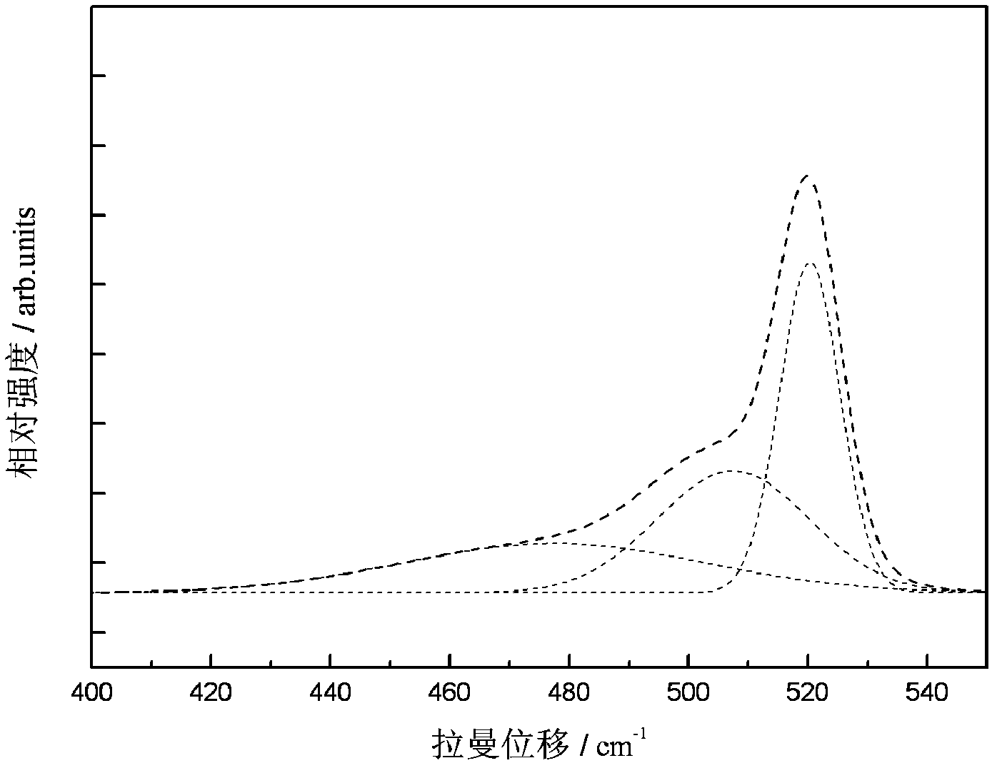
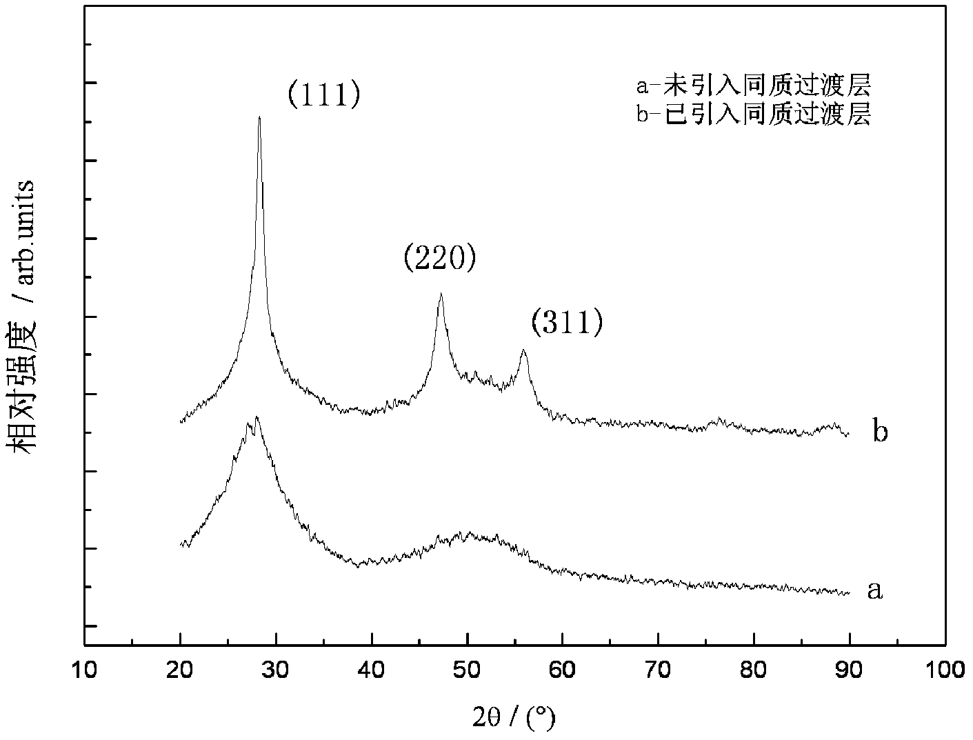
[0052] Common glass slides are used as the substrate, followed by ultrasonic cleaning with acetone and alcohol. After drying, they are placed on the sample table in the vacuum chamber of the ion beam magnetron sputtering composite coating equipment. The surface is cleaned by bombardment with low energy ion beams for 15 minutes before coating. Then an ion beam is used to assist the deposition of a silicon homogenous transition layer with a thickness of 68nm, that is, Ar with 2.5keV energy in use + While ion beam sputtering polycrystalline Si target, use another beam of Ar with energy of 30keV + Th...

Embodiment 3

[0057] The device described in Example 1 is used to realize a method of the present invention for preparing a microcrystalline silicon film by a two-step ion beam magnetron sputtering method:

[0058] Pulse magnetron sputtering deposition of microcrystalline silicon film, the target is polycrystalline silicon, the background vacuum is ≤1×10 -4 Pa, the hydrogen volume concentration is 80%.

[0059] Use ordinary glass slides as the substrate, followed by ultrasonic cleaning with acetone and alcohol. After drying, they are placed on the sample table in the vacuum chamber of the ion beam magnetron sputtering composite coating equipment. The surface is cleaned by bombardment with low energy ion beams for 15 minutes before coating. Then use 3.5keV Ar + Ion beam sputtering a polycrystalline Si target to deposit a silicon homogenous transition layer with a thickness of 117nm. After the transition layer is deposited, without breaking the vacuum, the sample table is transferred from the ion ...


PUM

PropertyMeasurementUnit
Thicknessaaaaaaaaaa

Abstract

The invention belongs to the technical field of microcrystalline silicon films for solar batteries, particularly relates to a method for preparing the microcrystalline silicon film by a two-step method of ion beam and magnetron sputtering and a device for coating a composite film by the ion beam and the magnetron sputtering. The method comprises the following steps: (1) ion beam coating: sputtering a silicon target on a substrate by ion beam sputtering (IBS) deposition or ion beam assisted deposition (IBAD), pre-depositing a silicon homogeneous transition layer, wherein the silicon homogeneous transition layer is 50-200nm in thickness; and (2) magnetron sputtering coating: depositing a silicon film on the silicon homogeneous transition layer by the magnetron sputtering. The method for preparing the microcrystalline silicon film can fully improve the crystalline ratio of the microcrystalline silicon film, at the same time can effectively reduce the internal stress between the film and the substrate and increase the bonding strength between the film and the substrate; and the method is realized through the device for coating the composite film by the ion beam and the magnetron sputtering and finished in a same vacuum room, so as to save equipment cost.

Description

Technical field [0001] The invention belongs to the technical field of microcrystalline silicon thin films for solar cells, and specifically relates to a method and device for preparing microcrystalline silicon thin films, and can also be applied to other fields where thin films are deposited on heterogeneous substrates to improve film adhesion and crystallinity. Background technique [0002] Silicon film is regarded as the core material of thin-film solar cells and has attracted more and more attention. The currently prepared silicon thin films mainly exist in amorphous form, but amorphous silicon thin-film photovoltaic cells have problems such as low conversion efficiency and efficiency degradation caused by the SW effect. Microcrystalline silicon thin films are a kind of nano-silicon crystals embedded in The materials in the amorphous network have high electrical conductivity, high mobility electrical properties and excellent optical stability. The preparation of microcrystall...

Claims


Application Information

Patent Timeline
IPC IPC(8): C23C14/35C23C14/46C23C14/06
Inventor 周灵平梁凤敏彭坤朱家俊李德意李绍禄
Owner HUNAN UNIV
Learn More