Supercharge Your Innovation With Domain-Expert AI Agents!

Periodic subwavelength metal structure on the surface of light-emitting diode and its preparation method

A technology of light-emitting diodes and sub-wavelength structures, applied in electrical components, circuits, semiconductor devices, etc., can solve the problems of undisclosed specific size preparation methods of metal structures, obvious luminous enhancement effects, and complicated preparation processes, and achieves improvement of internal quantum efficiency. and external quantum efficiency, improve external quantum efficiency, enhance the effect of luminous efficiency

Inactive Publication Date: 2014-10-15
UNIV OF ELECTRONICS SCI & TECH OF CHINA
View PDF6 Cites 0 Cited by
  • Summary
  • Abstract
  • Description
  • Claims
  • Application Information

AI Technical Summary

Problems solved by technology

However, this patent application does not disclose the specific dimensions and specific preparation methods of the metal structure, so that it is difficult for those skilled in the art to implement
Another example is the application of SPPs to photoluminescent materials (PL) in the Chinese Utility Model Patent Application No. 201120030792.9, which discloses a metal structure and a method for preparing the metal structure, but this method is mainly used for photoluminescent materials. LED is mainly electroluminescent, so the method is difficult to be directly applied to LED. The difficulty of the preparation method of the metal structure disclosed in this patent is: for the metal subwavelength periodic structure, the luminescence enhancement effect is obvious, but the preparation process is complicated and the cost is too high; and The non-periodic rough structure is prepared by a relatively simple method, and its enhancement effect is not satisfactory compared with the former

Method used


Image

  • Periodic subwavelength metal structure on the surface of light-emitting diode and its preparation method
  • Periodic subwavelength metal structure on the surface of light-emitting diode and its preparation method
  • Periodic subwavelength metal structure on the surface of light-emitting diode and its preparation method

Examples


Embodiment 1

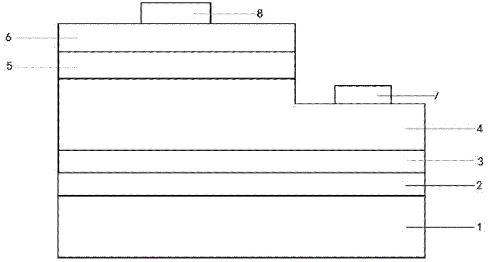
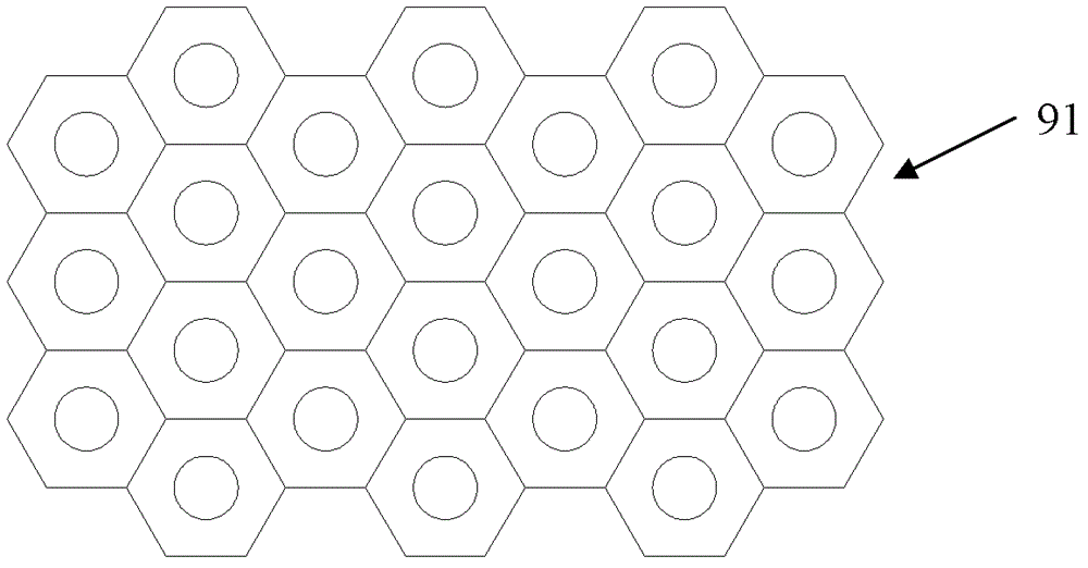
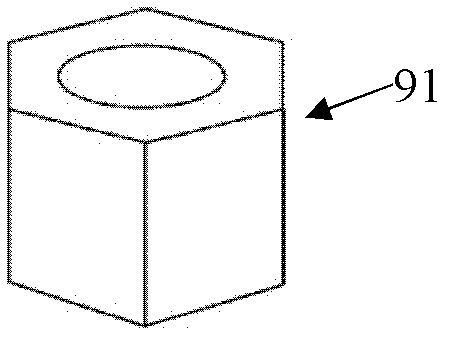
[0049] Embodiment 1: the anodic aluminum oxide (AAO) film structure used in this scheme is as follows figure 2 and shown in Figure 3. A self-made anodizing device was used for the preparation. The method for preparing the metal periodic sub-wavelength structure on the surface of the light-emitting diode comprises the following steps:

[0050] Step 1: Preparation of AAO thin film. The specific process is as follows:

[0051] Step 11: Pretreatment of aluminum flakes (99.999% pure, 0.5mm×50mm×100mm in size). Annealing, oil removal, oxide layer removal, and electropolishing are successively performed.

[0052] Step 12: An anodizing process. Using oxalic acid as electrolyte solution, lead as cathode, aluminum as anode, cooling by circulating water, magnetic stirring, steady flow control. The concentration of oxalic acid is 0.3mol / L, and the steady flow control is adopted: adjust the voltage to keep the current at 0.3-0.5A, the electrolysis temperature is 20-30°C, and the oxi...

Embodiment 2

[0065] Embodiment 2: The preparation method of the metal periodic sub-wavelength structure on the surface of the light-emitting diode comprises the following steps:

[0066] Step 1: Preparation of AAO thin film. The preparation of the AAO film in this example is the same as that described above.

[0067] Step 2: Fabrication of the isolation layer 93 .

[0068] On the surface of the InGaN light-emitting diode, the plasma-enhanced chemical vapor deposition (PECVD) method is used to deposit SiN with a thickness of 20-30nm. x The anti-reflection film is used as the isolation layer 93, and the process conditions for deposition are: the pre-vacuum degree of the reaction chamber is -3 Pa, as silane (SiH 4 ) and ammonia (NH 3 ) as the plasma gas source, the gas pressure during deposition is 60-80Pa, the temperature is 200°C-300°C (preferably 250°C), the RF power frequency is 10-15MHz (preferably 13.56MHz), and the output power is 0.2W / cm 2 .

[0069] Step 3: Fabrication of the na...


PUM

PropertyMeasurementUnit
pore sizeaaaaaaaaaa
thicknessaaaaaaaaaa
thicknessaaaaaaaaaa

Abstract

The invention relates to a metal periodic sub-wavelength structure on the surface of a light-emitting diode and a preparation method thereof. The metal periodic sub-wavelength structure on the surface of the light-emitting diode is provided with a metal periodic sub-wavelength structure on the P-type GaN layer and the N-type GaN layer of the semiconductor light-emitting diode that are exposed and not covered by the N electrode and the P electrode. The metal periodic sub-wavelength structure includes an isolation layer, a nano-metal lattice layer and a protective layer from bottom to top, the isolation layer is attached on the P-type GaN layer, the isolation layer is SiNx anti-reflection film, the The protective layer is a SiO2 or SiNx or ZnO protective film, the nano-metal lattice layer is a metal nano-lattice, the diameter of the nano-dots is 50-100nm, the distance between the nano-dots is 250-500nm, and the period of the lattice is 350-500nm , the thickness of the nano-dot is 100-300nm. The beneficial effect of the invention is that the total reflection is reduced through the surface non-smooth structure, and the external quantum efficiency can be greatly improved.

Description

technical field [0001] The invention belongs to the field of light-emitting diode technology (LED), in particular to the field of light-emitting diode technology enhanced by surface plasmon polaritons (SPPs, Surface Plasmon Polaritons) excited by surface metal periodic subwavelength structures. Background technique [0002] Replacing traditional light sources with LEDs is an effective way for countries to find energy-saving, low-consumption and environmentally friendly lighting. At present, bright LED light sources that can emit ultraviolet, blue, green and red light have been developed on the basis of InGaN (indium gallium nitride)-based quantum wells, and have been widely used in LCD backlight, lighting and traffic lights. However, due to constraints such as low luminous efficiency and other factors, the current manufacturing cost of LEDs for lighting in lumens is still much higher than that of fluorescent lamps. In addition, the higher the luminous efficiency, the less h...

Claims


Application Information

Patent Timeline
Patent Type & Authority Patents(China)
IPC IPC(8): H01L33/40H01L33/00
Inventor 林祖伦宋科田祁康成曹贵川
Owner UNIV OF ELECTRONICS SCI & TECH OF CHINA
Features
  • R&D
  • Intellectual Property
  • Life Sciences
  • Materials
  • Tech Scout
  • Unparalleled Data Quality
  • Higher Quality Content
  • 60% Fewer Hallucinations
Learn More