
Insulated gate bipolar transistor (IGBT) with low-conductivity saturation voltage drop and manufacturing method for IGBT

A low-conduction, semiconductor technology, used in semiconductor/solid-state device manufacturing, semiconductor devices, electrical components, etc., can solve problems such as the increase of sheet processing equipment, improve short-circuit current withstand capacity, reduce resistivity, and enhance impact resistance. Effect

Active Publication Date: 2012-07-11
WUXI NCE POWER
View PDF4 Cites 13 Cited by
  • Summary
  • Abstract
  • Description
  • Claims
  • Application Information

AI Technical Summary

Problems solved by technology

However, the price, process complexity and fragmentation rate of thin wafer processing equipment will increase significantly with the increase of semiconductor wafer size and the thinning of semiconductor wafer thickness, which has become an important bottleneck for further improving the cost performance of IGBT products. An important reason for the delay in promoting production on larger wafer sizes (such as 12 inches)

Method used


Image

  • Insulated gate bipolar transistor (IGBT) with low-conductivity saturation voltage drop and manufacturing method for IGBT
  • Insulated gate bipolar transistor (IGBT) with low-conductivity saturation voltage drop and manufacturing method for IGBT
  • Insulated gate bipolar transistor (IGBT) with low-conductivity saturation voltage drop and manufacturing method for IGBT

Examples


Embodiment Construction

[0078] The present invention will be further described below in conjunction with specific drawings and embodiments.

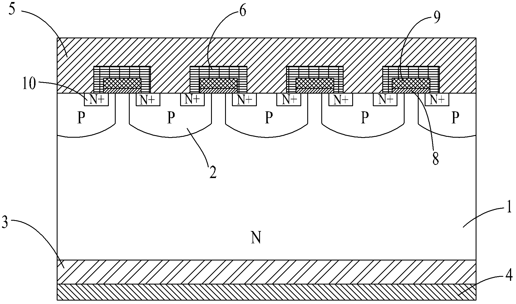
[0079] Such as image 3 , Figure 4 , Figure 5 , Image 6 , Figure 7 with Figure 18 Shown: the present invention takes N-type IGBT as an example to illustrate the structure and corresponding working principle of the present invention.

[0080] Such as Figure 5 As shown, in the top view of the IGBT device, the device includes an active region 15 and a terminal protection region 16 surrounding the active region 15; the active region 15 includes conductive polysilicon 9 arranged in parallel strips, so The conductive polysilicon 9 separates the P well layer 2 in the active region 15 into a P well layer first region 11 and a P well layer second region 12, and the P well layer first region 11 and the P well layer second region 12 alternately and regularly arranged, the first region 11 of the P well layer is provided with an N+ implantation region 10, and a...


PUM


Abstract

The invention relates to an insulated gate bipolar transistor (IGBT) with low-conductivity saturation voltage drop and a manufacturing method for the IGBT. A second conductive type layer is arranged in an active region and partitioned into a plurality of second conductive type layer first regions and a second conductive type layer second regions by conductive polysilicon and insulated gate medium layers; an insulation medium layer is covered on the first main surface of a semiconductor substrate; first conductive type injection regions are symmetrically arranged in the second conductive type layer first regions and contacted with the corresponding insulated gate medium layers; emitter contact holes are formed above the second conductive type layer second regions, pass through the insulation medium layer and extend to the first main surface; emitter metal layers are filled in the emitter contact holes and covered on the insulation medium layer; and the emitter metal layers are in ohm contact with the second conductive type layer first regions. The IGBT has relatively low saturation voltage drop Vcesat and relatively high impact resistance.

Description

technical field [0001] The invention relates to an IGBT device and a manufacturing method thereof, in particular to an IGBT with low conduction saturation voltage drop and a manufacturing method thereof, belonging to the technical field of power semiconductor devices. Background technique [0002] The current main device structure types of IGBT (Insulated Gate Bipolar Transistor) include: Punch Through IGBT (Punch Through IGBT, referred to as PT-IGBT), Non Punch Through IGBT (Non Punch Through IGBT, referred to as NPT-IGBT) and field stop type IGBT (Field Stop IGBT, referred to as FS-IGBT), the main structural difference among the three is to set different back collector structures and different semiconductor drift region thicknesses. [0003] PT-IGBT is an earlier IGBT structure. Due to the use of a thick back collector structure, its high proportion of hole injection current is not conducive to the switching power loss of the device and the temperature characteristics of t...

Claims


Application Information

Patent Timeline
Patent Type & Authority Applications(China)
IPC IPC(8): H01L29/739H01L29/06H01L21/331
Inventor 朱袁正叶鹏
Owner WUXI NCE POWER
Learn More