Chemical mechanical planarization method and manufacturing method of gate last

A planarization method and chemical-mechanical technology, applied in semiconductor/solid-state device manufacturing, semiconductor devices, electrical components, etc., can solve problems such as process obstacles, drop, device short-circuit, etc., and achieve the effect of avoiding short-circuit defects

Active Publication Date: 2015-06-24
INST OF MICROELECTRONICS CHINESE ACAD OF SCI
View PDF3 Cites 0 Cited by
  • Summary
  • Abstract
  • Description
  • Claims
  • Application Information

AI Technical Summary

Problems solved by technology

[0005] However, the problem is that due to the high density of the polysilicon gate 11, and the gate height difference exists on the substrate surface before the deposition of the silicon oxide spacer 13, which is about 1000A to 1800A, the polysilicon gate 11 after the silicon oxide spacer 13 is deposited The thickness difference h of the silicon oxide isolation layer 13 between the top and the source and drain regions (not shown in the figure) can reach 1000A to 4000A, or even more
The conventional silicon oxide CMP process usually cannot effectively eliminate such a large thickness drop, and it will be inherited until the grinding process of the silicon oxide isolation layer 13 is completed as the grinding process progresses, such as figure 2 As shown, this drop causes pits 14 to be formed in the remaining silicon oxide isolation layer 13 between the polysilicon gates 11, and it is difficult to repair even the CMP of the silicon nitride isolation layer 12 in the next step. It is possible to further enlarge the pit 14 of this silicon oxide isolation layer 13
like image 3 and Figure 4 As shown, the pits 14 of the silicon oxide isolation layer are also filled with metal materials, which will directly cause huge obstacles to the process in the subsequent metal gate CMP process, greatly compress the adjustment space of the process, and easily cause gaps between the gates. Metal residues, causing short circuits in the device

Method used


Image

  • Chemical mechanical planarization method and manufacturing method of gate last
  • Chemical mechanical planarization method and manufacturing method of gate last
  • Chemical mechanical planarization method and manufacturing method of gate last

Examples


Embodiment 1

[0044] Figure 5 It is a flow chart of the chemical mechanical planarization method in this embodiment, Figure 6 to Figure 8 It is a schematic diagram of the chemical mechanical planarization method in this embodiment.

[0045] As shown, the method includes:

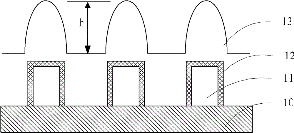
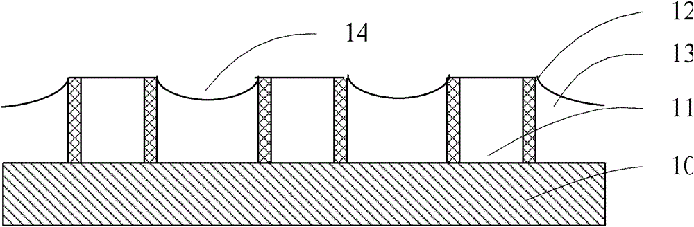
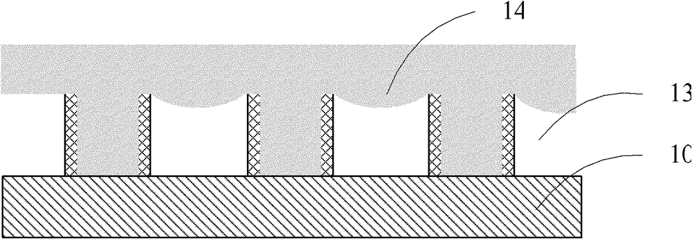
[0046] Step S1: if Figure 6As shown, a substrate 100 with a gate 101 and source and drain regions (not shown) on both sides of the gate 101 is provided, and the gate 101 and the source and drain regions are covered with an isolation layer 102, wherein the isolation layer 102 includes a raised portion 102a located above the gates and a recessed portion 102b located on the surface of the substrate between the gates 101 .

[0047] Step S2: Perform a selective doping process on the isolation layer 102, so that only the raised portion 102a is doped; preferably, in this embodiment, the selective doping process is an ion implantation process, refer to Figure 6 , the mask layer 103 covers the recessed portion 102b of the ...

Embodiment 2

[0055] This embodiment takes a typical metal gate-last manufacturing method of 32nm technology as an example to illustrate another implementation of the chemical mechanical planarization method. Figure 9 to Figure 16 It is a schematic diagram of the manufacturing method of the rear metal grid in this embodiment.

[0056] Such as Figure 9 As shown, a substrate 200 is provided. The substrate 200 includes a dummy gate 201, a gate oxide layer (not shown in the figure) and source and drain regions (not shown in the figure) on both sides of the dummy gate 200. The dummy gate 201 and The source and drain regions are sequentially covered with a first isolation layer 208 and a second isolation layer 202 .

[0057] Specifically, the substrate 200 can be a bulk material composed of elemental semiconductors or components, such as silicon or silicon germanium with a single crystal, polycrystalline or amorphous structure, or a bulk material composed of compound semiconductors, such as si...


PUM


Abstract

Methods for chemical mechanical planarization (CMP) and fabricating gate last are provided. The method for CMP including: Substrate with gate and with source and drain on both sides of the gate is provided. The gate and the source and drain are covered with an insulate layer which includes protruding part lying on the gate and concave part lying on the surface of substrate between the gates. Selective doping process is performed on the insulate layer where only the protruding part of the insulate layer is doped. CMP process is performed on the doped substrate to remove the protruding part and planarize the surface of the substrate. By performing selective doping process on the insulate layer where only the protruding part of the insulate layer is doped, the method can enhance chemical corrosion effect of polishing slurry on the material of protruding part in the CMP process, and increase the removing rate of the protruding material in the CMP process, thus improve uniformity in the chip during the polishing process. Furthermore, during the process of forming gate last, there will not be remaining metal in the insulate layer between the gates, which can avoid short circuit defect of the device.

Description

technical field [0001] The invention relates to the technical field of integrated circuit manufacturing, in particular to a chemical mechanical planarization method. Background technique [0002] With the increasing demand for high integration and high performance of VLSI, semiconductor technology is developing towards technology nodes with feature sizes of 45 nanometers or even smaller. Due to the successful application of the high-K / metal gate process on the 45nm technology node, this process has become an indispensable key process module for the technology node below 30nm. At present, in terms of mass production of 45nm and 32nm chips, only Intel, which adheres to the high-K / gate last process, has achieved success. In recent years, Samsung, TSMC, Infineon, etc. Industry giants will also shift their development focus from high-K / gate first to gate last. [0003] For the gate last process, the development of the chemical mechanical planarization (CMP) process is considere...

Claims


Application Information

Patent Timeline
Patent Type & Authority Patents(China)
IPC IPC(8): H01L21/3105H01L21/265H01L21/28
CPCH01L21/31053H01L29/66545
Inventor 杨涛刘金彪贺晓彬赵超陈大鹏
Owner INST OF MICROELECTRONICS CHINESE ACAD OF SCI
Why Eureka
Try Eureka