Organic EL display device and method for production of the same
An electroluminescence display and display device technology, applied in electroluminescence light sources, electric light sources, luminescent materials, etc., can solve the problems of deterioration of device characteristics, reduced uniformity life, increased driving voltage, etc., and improved electron injection efficiency. , the effect of improving the luminous efficiency and increasing the amount of electrons
- Summary
- Abstract
- Description
- Claims
- Application Information
AI Technical Summary
Problems solved by technology
Method used
Image

Examples
Embodiment approach
[0041] 1. First embodiment (organic EL display device in which electron injection / transport layers are formed on light emitting layers of each color)
[0042] 2. Second embodiment (organic EL display device in which a hole blocking layer is formed between each color light emitting layer and an electron injection / transport layer)
no. 1 approach
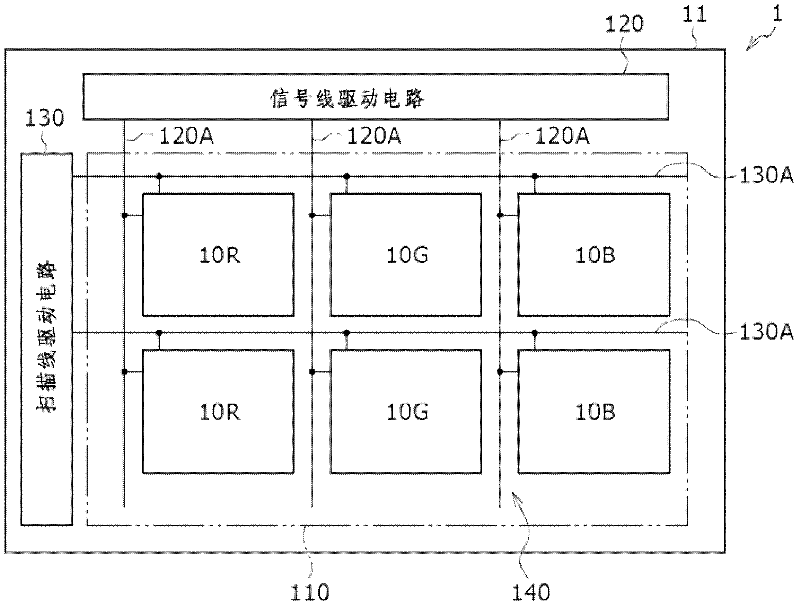
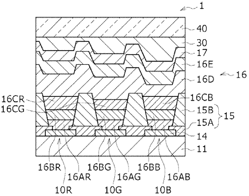
[0044] figure 1 The structure of the organic EL display device 1 according to the first embodiment of the present invention is shown. The organic EL display device 1 is designed to be used as an organic EL television. It consists of a substrate 11 and a display area 110 formed on the substrate. The display area 110 includes red organic EL elements 10R, green organic EL elements 10G, and blue organic EL elements 10B arranged in a matrix. These organic EL elements will be described in detail later. Along both sides of the display area 110 are provided a signal line driver circuit 120 and a scan line driver circuit 130 serving as drivers for screen display.
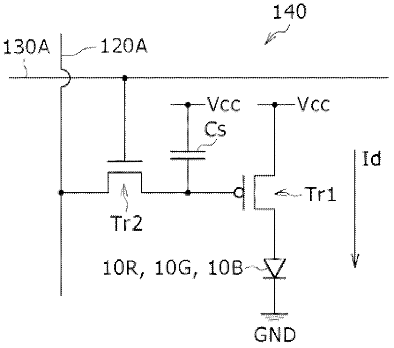
[0045] A pixel driving circuit 140 is provided in the display area 110, figure 2 A pixel driver circuit 140 is shown. The pixel driving circuit 140 is an active type driving circuit formed under the lower electrode 14 to be described later. Each pixel driving circuit 140 is composed of a driving transistor Tr1, a writin...
no. 2 approach
[0205] The second embodiment will be described below. The same constituent elements as those of the first embodiment are given the same reference numerals and will not be described again. There are no drawings for showing the overall structure of the organic EL display device according to the second embodiment of the present invention. Like the first embodiment, the organic EL display device according to the second embodiment has a display area composed of red organic EL elements 20R, green organic EL elements 20G, and blue organic EL elements arranged in a matrix on a substrate 11. Element 20B constitutes. A pixel driving circuit is provided in the display area.
[0206] The red organic EL element 20R, the green organic EL element 20G, and the blue organic EL element 20B in the display area constitute a matrix form such that the red organic EL element 20R, the green organic EL element 20G, and the blue organic EL element 20B are adjacent to each other. Combined to form a p...
PUM
| Property | Measurement | Unit |
|---|---|---|
| Thickness | aaaaa | aaaaa |
| Thickness | aaaaa | aaaaa |
| Thickness | aaaaa | aaaaa |
Abstract
Description
Claims
Application Information
 - R&D
- Intellectual Property
- Life Sciences
- Materials
- Tech Scout
- Unparalleled Data Quality
- Higher Quality Content
- 60% Fewer Hallucinations
Browse by: Latest US Patents, China's latest patents, Technical Efficacy Thesaurus, Application Domain, Technology Topic, Popular Technical Reports.
© 2025 PatSnap. All rights reserved.Legal|Privacy policy|Modern Slavery Act Transparency Statement|Sitemap|About US| Contact US: help@patsnap.com