
Patsnap Eureka
For R&D, Patsnap Eureka makes reading and utilizing patents & technical documents easy.
Patsnap Eureka AIR
Designed for self-driven R&D workflows. Generate viable solutions, solve complex R&D challenges, empower your innovation with AI.

Patsnap Eureka Materials
Designed for material experts only. Revolutionize your material R&D, from search, analyze, to developing new materials.

TechResearch
Generate reliable direction feasibility study reports for your R&D in just a few steps.

TechSeek
Discover and master advanced knowledge NOW. Basics, ideas, possibilities, all at once.

TechMind
As an expert in R&D Theories, TechMind can generates customized viable solutions instantly.

TechRisk
Analyze your overall solution with one click, know your potential R&D risks in advance.

TechMonitor
Get weekly tech updates, stay abreast of the latest tech innovations and key insights.
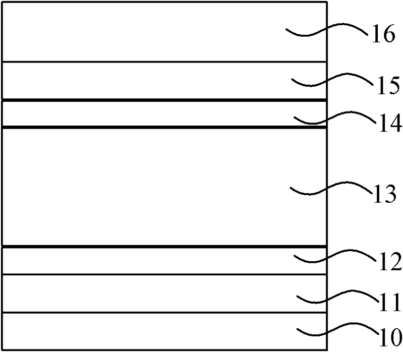
Thin film solar cell and formation method thereof
A technology for solar cells and thin films, which is applied to circuits, photovoltaic power generation, electrical components, etc., can solve the problems of contaminating the I-type amorphous silicon layer 13, reducing the photoelectric conversion efficiency of thin-film solar cells, and reducing the band gap width of thin-film solar cells, etc. Achieve the effect of improving photoelectric conversion efficiency, increasing band gap width, and reducing pollution
- Summary
- Abstract
- Description
- Claims
- Application Information
AI Technical Summary
Problems solved by technology
Method used
Image


Examples
Embodiment Construction
[0036] In order to make the above objects, features and advantages of the present invention more comprehensible, specific implementations of the present invention will be described in detail below in conjunction with the accompanying drawings.
[0037] In the following description, many specific details are set forth in order to fully understand the present invention, but the present invention can also be implemented in other ways than here, so the present invention is not limited by the specific embodiments disclosed below.
[0038] As mentioned in the background section, in the prior art, both the P-type semiconductor layer and the N-type semiconductor layer are uniformly doped. In order to reduce the pollution to the I-type semiconductor layer, it is necessary to reduce the doping ion concentration of the P-type semiconductor layer and the N-type semiconductor layer; but in order to increase the bandgap width, it is necessary to increase the doping of the P-type semiconducto...
PUM
 Abstract
Description
Claims
Application Information
 - R&D Engineer
- R&D Manager
- IP Professional
- Industry Leading Data Capabilities
- Powerful AI technology
- Patent DNA Extraction
Browse by: Latest US Patents, China's latest patents, Technical Efficacy Thesaurus, Application Domain, Technology Topic, Popular Technical Reports.
© 2024 PatSnap. All rights reserved.Legal|Privacy policy|Modern Slavery Act Transparency Statement|Sitemap|About US| Contact US: help@patsnap.com