Cubic boron nitride piezoelectric film surface acoustic wave device and preparation method thereof

A surface acoustic wave device, boron nitride piezoelectric technology, applied in the direction of electrical components, impedance networks, etc., to achieve high frequency effects

Inactive Publication Date: 2012-05-02
TIANJIN UNIVERSITY OF TECHNOLOGY
View PDF3 Cites 6 Cited by
  • Summary
  • Abstract
  • Description
  • Claims
  • Application Information

AI Technical Summary

Problems solved by technology

[0005] However, diamond itself is not a piezoelectric material and cannot perform energy conversion between electromagnetic waves and surface acoustic waves, so a piezoelectric film (such as ZnO, LiNbO, etc.) needs to be deposited on it. 3 , AlN, c-BN, etc.), made of multilayer film SAW devices

Method used


Image

  • Cubic boron nitride piezoelectric film surface acoustic wave device and preparation method thereof
  • Cubic boron nitride piezoelectric film surface acoustic wave device and preparation method thereof
  • Cubic boron nitride piezoelectric film surface acoustic wave device and preparation method thereof

Examples


Embodiment 1

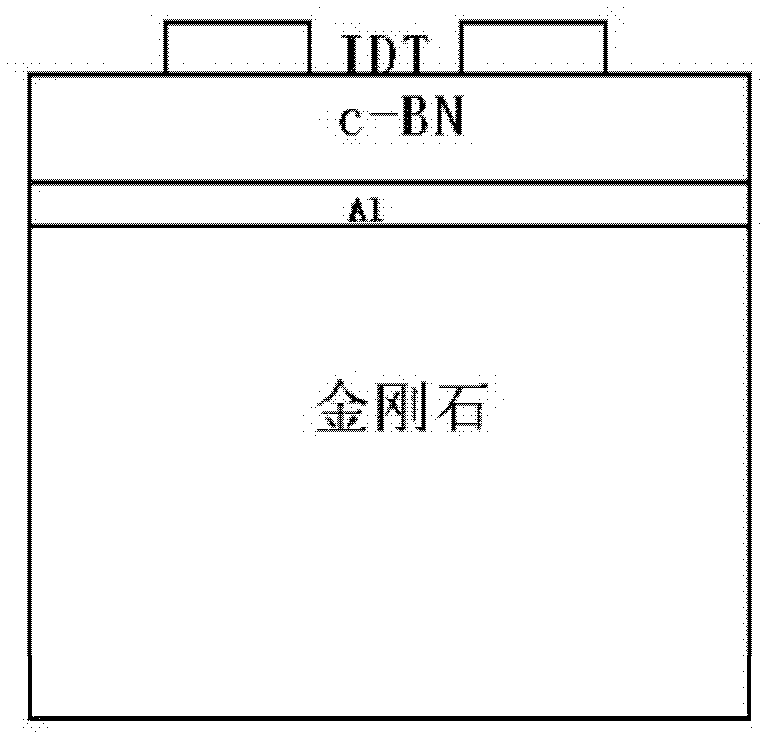
[0028] A method for preparing a cubic boron nitride piezoelectric thin film surface acoustic wave device, comprising the steps of:

[0029] 1) Prepare nano-Al film on the surface of nano-CVD diamond substrate by DC magnetron sputtering:

[0030] Nano-Al films were prepared on the surface of nano-CVD diamond substrates using a DC magnetron sputtering system. The specific process parameters were: the background vacuum was 3.3×10 -4 Pa, the rotation speed of the substrate turntable is 20 rpm, the substrate temperature is room temperature, the sputtering power is 50w, the argon gas flow rate is 20sccm, the working pressure is 1.0Pa, the target base distance is 6.5cm, and the deposition time is 12 minutes;

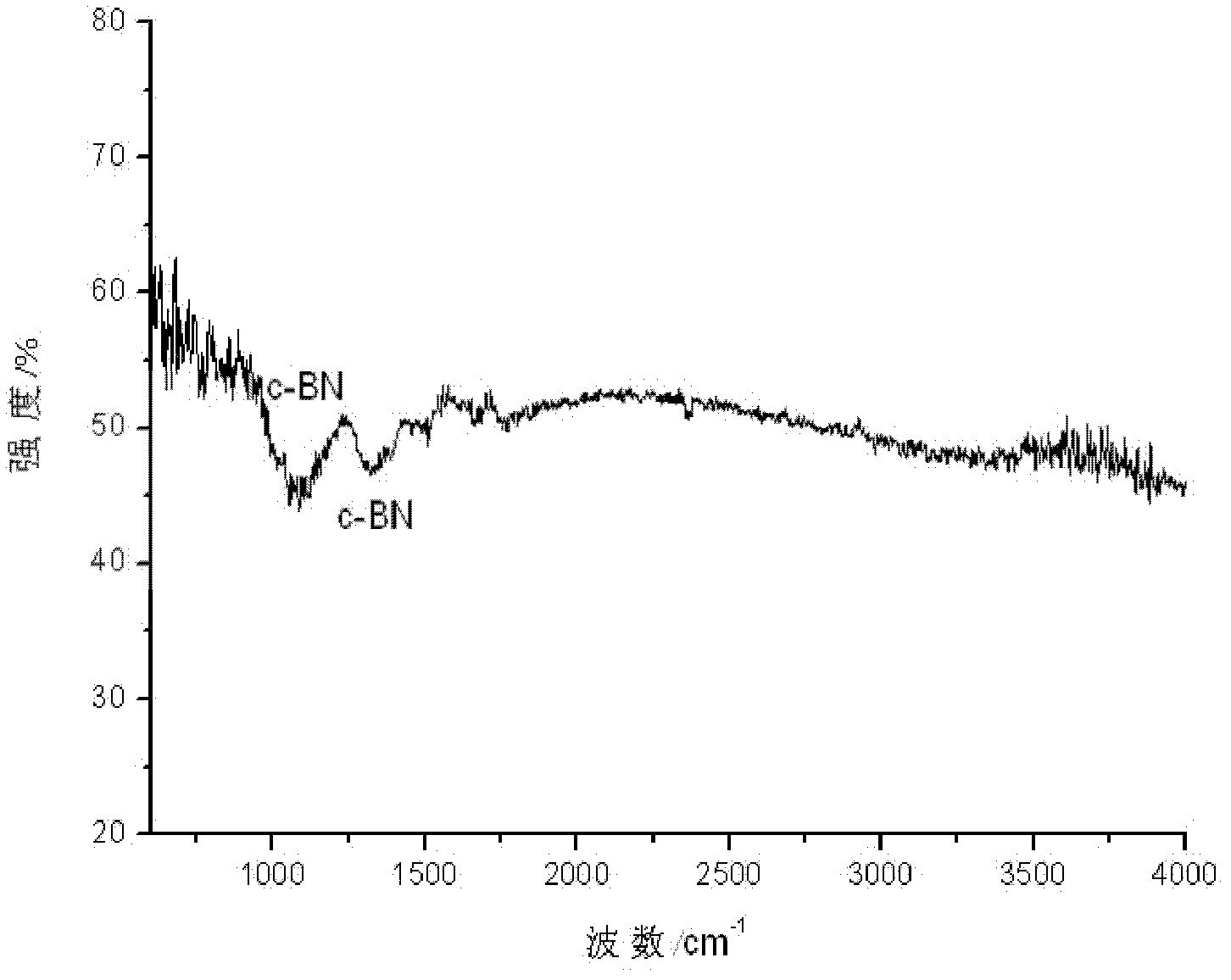
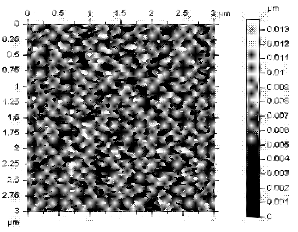
[0031] 2) Prepare nano-cubic boron nitride c-BN film on the surface of nano-Al film by radio frequency magnetron sputtering method:

[0032] Using radio frequency magnetron sputtering system to deposit nano-cubic boron nitride c-BN film can be realized at low temperature and l...

Embodiment 2

[0038] A method for preparing a cubic boron nitride piezoelectric thin film surface acoustic wave device, comprising the steps of:

[0039] 1) Prepare nano-Al film on the surface of nano-CVD diamond substrate by DC magnetron sputtering:

[0040] Nano-Al films were prepared on the surface of nano-CVD diamond substrates using a DC magnetron sputtering system. The specific process parameters were: the background vacuum was 3.3×10 -4 Pa, the rotation speed of the substrate turntable is 20 rpm, the substrate temperature is room temperature, the sputtering power is 50w, the argon gas flow rate is 18sccm, the working pressure is 1.0Pa, the target base distance is 6.5cm, and the deposition time is 12 minutes;

[0041] 2) Prepare nano-cubic boron nitride c-BN film on the surface of nano-Al film by radio frequency magnetron sputtering method:

[0042] Using radio frequency magnetron sputtering system to deposit nano-cubic boron nitride c-BN film can be realized at low temperature and l...


PUM

PropertyMeasurementUnit
Film thicknessaaaaaaaaaa

Abstract

The invention provides a cubic boron nitride piezoelectric film surface acoustic wave (SAW) device which is an IDT / c-BN / Al / diamond multilayer film structure and is composed of a diamond substrate, an interface layer nano-aluminum film and a layer of nano-cubic boron nitride (c-BN) piezoelectric film formed on a surface of the nano-aluminum film. A preparation method of the device comprises the following steps: (1) employing a direct current magnetron sputtering method to deposit the nano-aluminum film on a nano-CVD diamond substrate surface; (2) employing a radio frequency magnetron sputtering method to deposit the nano-cubic boron nitride (c-BN) piezoelectric film on a surface of the nano-aluminum film; (3) preparing an interdigital transducer (IDT) on a surface of the nano-cubic boron nitride (c-BN) piezoelectric film. The surface acoustic wave device can satisfy application requirements of various fields like the surface acoustic wave (SAW) device with high frequency (4.8 GHz or more), a high electromechanical coupling coefficient, large power (more than 8 w), low propagation loss and a low frequency temperature coefficient, preparation technology is simple, application is easy, and popularization is facilitated.

Description

technical field [0001] The invention relates to a surface acoustic wave device, in particular to a cubic boron nitride piezoelectric film surface acoustic wave device and a preparation method thereof. Background technique [0002] With the rapid development of information and communication technology, high-frequency SAW filters have been widely used in the intermediate frequency (IF) filtering of third-generation digital mobile communication systems and high-frequency systems in recent years. However, the frequency band lower than 2.5 GHz has been fully occupied, so there is an urgent need for high-frequency surface acoustic wave devices of 2.5-10 GHz. In addition, mobile communication devices require devices to be miniaturized and capable of withstanding high power, so it is imminent to develop high-frequency (above 4.8 GHz) SAW devices. [0003] Conventional SAW materials such as quartz, LiNbO 3 , LiTaO 3 , ZnO, etc., the phase velocity of the surface acoustic wave is l...

Claims


Application Information

Patent Timeline
IPC IPC(8): H03H9/145H03H3/08
Inventor 陈希明孙连婕薛玉明郭燕阴聚乾张倩
Owner TIANJIN UNIVERSITY OF TECHNOLOGY
Why Eureka
Try Eureka