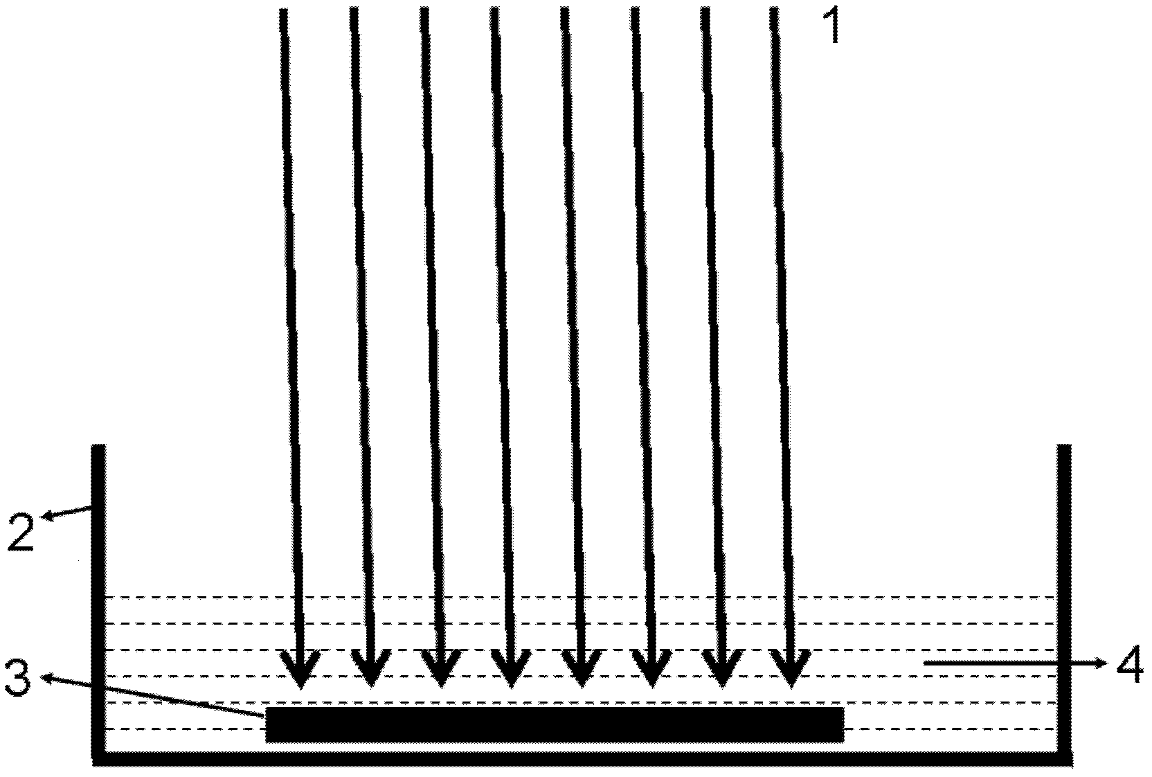
A method for wet roughening of gallium phosphide window layer of light-assisted red LED
A gallium phosphide and window layer technology, applied in semiconductor devices, electrical components, circuits, etc., can solve the problems of unfavorable light extraction, cumbersome steps, and high cost of corrosion structures, and achieve improved light extraction efficiency, large processing area, and easy operation Effect
- Summary
- Abstract
- Description
- Claims
- Application Information
AI Technical Summary
Problems solved by technology
Method used
Image
Examples
Embodiment 1
[0029] Taking a 2-inch GaAs-based front-mounted red LED epitaxial wafer as an example to illustrate the implementation method of the present invention:
[0030] (1) The structure of the GaAs-based front-loading red LED epitaxial wafer from bottom to top is GaAs substrate, n-GaAs confinement layer, multi-quantum well active light-emitting region, p-GaAs confinement layer, and GaP window layer.
[0031] (2) Put the GaP layer of the red LED epitaxial wafer upwards into the polytetrafluoroethylene reaction vessel.
[0032] (3) Turn on the 532nm light source so that the power density irradiated on the surface of the epitaxial wafer is 1 μW / cm 2 .
[0033] (4) Add a mixed solution of 1% hydrofluoric acid and 0.1% hydrogen peroxide into the reaction vessel until the liquid level is above the surface of the epitaxial wafer.
[0034] (5) Stand for reaction for 3 hours.
[0035] (6) The cleaning process after the corrosion is completed is ultrasonic cleaning with high-purity water fo...
Embodiment 2
[0038] Take the 2-inch AlGaInP-based front-loading red LED epitaxial wafer as an example to illustrate the realization method of the present invention, the 2nd and 7th steps are the same as the example 1, the difference is:
[0039] (1) The structure of the AlGaInP-based front-loading red LED epitaxial wafer from bottom to top is gallium arsenide substrate, n-AlGaInP confinement layer, multi-quantum well active light-emitting region, p-AlGaInP confinement layer, and GaP window layer.
[0040] (2) Turn on the 450nm light source so that the power density irradiated on the surface of the epitaxial wafer is 100mW / cm 2 .
[0041] (3) Add a mixed solution of 40% hydrofluoric acid and 50% potassium ferricyanide into the reaction vessel until the liquid level is above the surface of the epitaxial wafer.
[0042] (4) Stand for reaction for 3 minutes.
[0043] (5) The cleaning process after the corrosion is completed is ultrasonic cleaning with high-purity water for 15 minutes, ultrason...
Embodiment 3
[0045] 2-inch AlGaInP-based front-loading red LED epitaxial wafer is taken as an example to illustrate the realization method of the present invention, and the first, second, and seventh steps are the same as in Example 2, except that:
[0046] (1) Turn on the 480nm light source so that the power density irradiated on the surface of the epitaxial wafer is 20mW / cm 2 .
[0047] (2) Add a mixed solution of 10% hydrofluoric acid and 20% potassium permanganate into the reaction vessel until the liquid level is above the surface of the epitaxial wafer.
[0048] (3) Stand for reaction for 12 minutes.
[0049] (4) The cleaning process after the corrosion is completed is ultrasonic cleaning with high-purity water for 20 minutes, ultrasonic cleaning with acetone for 20 minutes, and ultrasonic cleaning with ethanol for 10 minutes.
PUM
 Abstract
Description
Claims
Application Information
 - R&D
- Intellectual Property
- Life Sciences
- Materials
- Tech Scout
- Unparalleled Data Quality
- Higher Quality Content
- 60% Fewer Hallucinations
Browse by: Latest US Patents, China's latest patents, Technical Efficacy Thesaurus, Application Domain, Technology Topic, Popular Technical Reports.
© 2025 PatSnap. All rights reserved.Legal|Privacy policy|Modern Slavery Act Transparency Statement|Sitemap|About US| Contact US: help@patsnap.com


