Preparation method of n type GaSb ohmic contact having diffusion impervious layer Mo

A technology of ohmic contact and barrier layer, applied in the direction of laser components, electrical components, lasers, etc., can solve the problems of unfavorable ohmic contact, increased barrier height, low solubility, etc., and achieve the expansion of alloy temperature range and low specific contact resistance , the effect of improving reliability

Inactive Publication Date: 2011-11-23
CHANGCHUN UNIV OF SCI & TECH
View PDF1 Cites 2 Cited by
  • Summary
  • Abstract
  • Description
  • Claims
  • Application Information

AI Technical Summary

Problems solved by technology

Secondly, compared with other refractory metals such as Pt, Pa, Ni, Cr, W, etc., the work function is lower than that of Pt, Pa, Ni. When these high work function metals diffuse to the surface of GaSb, it will cause the metal and semiconductor contact The barrier height increases, which is not conducive to the formation of ohmic contacts, and the solubility of Mo in Au is relatively low

Method used


Image

  • Preparation method of n type GaSb ohmic contact having diffusion impervious layer Mo

Examples


Embodiment Construction

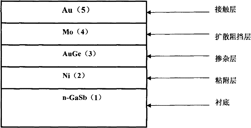
[0009] Such as figure 1 As shown, an n-GaSb-based device ohmic contact structure with a diffusion barrier layer Mo includes n-GaSb substrate (1), Ni adhesion layer (2), Au, Ge doped layer (3), Mo diffusion barrier layer (4), Au contact layer (5). The substrate (1) is a Te-doped GaSb substrate; the thickness of the Ni adhesion layer is 30nm (2); the thickness of the Au and Ge doped layer (Au88%, Ge12%) is 50nm (3); the thickness of the Mo diffusion barrier layer 60nm-100nm (4); Au contact layer 300nm (5);. Illustrate the present invention below in conjunction with example, the equipment that adopts is that the equipment that adopts is DISCOVERY--18 magnetron sputtering furnace. The substrate (1) is (100) orientation doped Te doping concentration is (3~7)×10 17 cm -3 n-GaSb crystal material with a mobility of 3500cm 2 / v·s(T=300K), thickness is 410μm, EPD≤8000 / cm 2 .

[0010] Sputtering the Ni adhesion layer (2), the gas flow rate is 20sccm, the input current is 0.2A; the...


PUM

PropertyMeasurementUnit
thicknessaaaaaaaaaa
thicknessaaaaaaaaaa
thicknessaaaaaaaaaa

Abstract

The invention provides a preparation method of an n type GaSb ohmic contact having a diffusion impervious layer Mo. According to the invention, a structure, which is in a form of Au / Mo / Au & Ge / Ni / n-GaSb from top to bottom, is employed. A diffusion impervious layer Mo is added between a contact layer Au and a doping layer Au & Ge; and the thickness of the diffusion impervious layer Mo is 60 nm to 100 nm; and thus an n type GaSb ohmic contact is formed. The beneficial effects of the method provided in the invention are as follows: a metallization system has low specific contact resistance, thereby extending an alloy temperature range; moreover, the metallization system also has a flattening surface morphology, so that reliability of a semiconductor laser device with an n-GaSb substrate is improved.

Description

technical field [0001] The invention relates to the technical field of semiconductor laser preparation technology, and belongs to the semiconductor laser chip technology. Background technique [0002] The III-V compound semiconductor material GaSb is due to its lattice constant matching with that of various ternary and quaternary III-V compound solid solutions with band gaps covering a wide spectral range of 0.8-4.3 μm, so GaSb It can be used as a substrate material to make lasers and detectors suitable for some infrared optical fiber transmission. The GaAs / GaSb solar cell developed with GaSb single crystal as the substrate has a conversion efficiency of more than 30%. At the same time, GaSb is also predicted to have a lattice-limited mobility greater than that of GaAs, which makes it have potential application prospects in making microwave devices. [0003] Regarding the n-GaSb-based ohmic contact metallization system, due to the characteristics of the n-GaSb substrate its...

Claims


Application Information

Patent Timeline
Patent Type & Authority Applications(China)
IPC IPC(8): H01S5/323
Inventor 李俊承王跃芦鹏王玉霞李林李再金李占国刘国军
Owner CHANGCHUN UNIV OF SCI & TECH
Why Eureka
Try Eureka