GaN base LED high reflectance electrode
An electrode, high-reflection technology, applied in circuits, electrical components, semiconductor devices, etc., can solve the problems of low contact resistance, less light absorption, and the inability of P-type electrodes to achieve low specific contact resistance, improve output power and thermal reliability. The effect of low light absorption and low light absorption
- Summary
- Abstract
- Description
- Claims
- Application Information
AI Technical Summary
Problems solved by technology
Method used
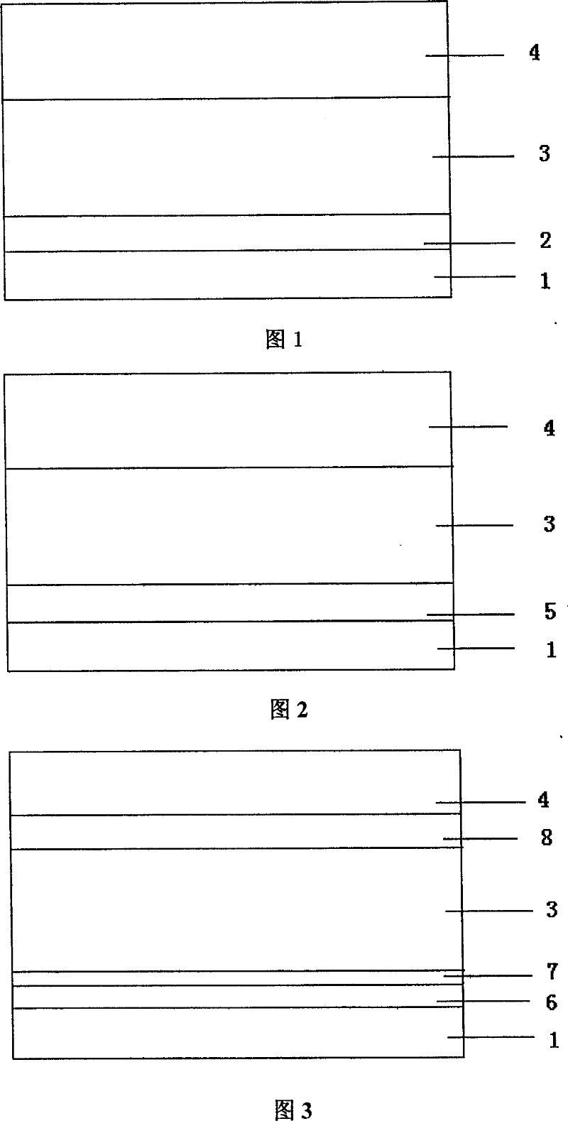
Image

Examples
Embodiment 1
[0016] 1) A 300 μm × 300 μm LED sample was prepared by the common metal-organic chemical vapor deposition (MOCVD) method, the P-GaN substrate thickness was 1.5 μm, and the Mg doping was 5 × 10 17 cm -3 ;
[0017] 2) The sample is cleaned by common chemical cleaning method: HCl: H 2 The surface of the GaN in the P region was cleaned with a solution of 1:1 O for 5 minutes, and then washed with deionized water for 5 times. After washing with dry N 2 air dry;
[0018] 3) Put the sample into the reaction chamber of the Denton Discovery550 sputtering station quickly, and pump the reaction chamber to 10 -5 Vacuum below Pa;
[0019] 4) On the semiconductor surface, a metal solid solution of Ni and Mg is plated at a rate of 1 Ȧ / s at 70°C as a contact layer, the thickness is 0.7nm, and the weight ratio of Mg is 10%; the purity of Ni is 4N (99.99%);
[0020] 5) Coating a layer of 0.6nm metal Pd on the Ni-Mg solid solution at a rate of 1 Ȧ / s at 60°C;
[0021] 6) The transmittance ...
Embodiment 2
[0028] 1) A 300 μm × 300 μm LED sample was prepared by the common metal-organic chemical vapor deposition (MOCVD) method, the P-GaN substrate thickness was 1.5 μm, and the Mg doping was 5 × 10 17 cm -3 ;
[0029] 2) The sample is cleaned by common chemical cleaning method: HCl: H 2 The surface of the GaN in the P region was cleaned with a solution of 1:1 O for 5 minutes, and then washed with deionized water for 5 times. After washing with dry N 2 air dry;
[0030] 3) Put the sample into the reaction chamber of the Denton Discovery550 sputtering station quickly, and pump the reaction chamber to 10-5 Vacuum below Pa;
[0031] 4) Plating a metal solid solution of Ni and Mg on the semiconductor surface at a rate of 1 Ȧ / s at 70°C as a contact layer, the thickness is 1nm, and the weight ratio of Mg is 8%; the purity of Ni is 4N (99.99%);
[0032] 5) Coating a layer of 0.6nm metal Pd on the Ni-Mg solid solution at a rate of 1 Ȧ / s at 60°C;
[0033] 6) The transmittance of the c...
Embodiment 3
[0040] 1) A 300 μm × 300 μm LED sample was prepared by the common metal-organic chemical vapor deposition (MOCVD) method, the P-GaN substrate thickness was 1.5 μm, and the Mg doping was 5 × 10 17 cm -3 ;
[0041] 2) The sample is cleaned by common chemical cleaning method: HCl: H 2 The surface of the GaN in the P region was cleaned with a solution of 1:1 O for 5 minutes, and then washed with deionized water for 5 times. After washing with dry N 2 air dry;
[0042] 3) Put the sample into the reaction chamber of the Denton Discovery550 sputtering station quickly, and pump the reaction chamber to 10 -5 Vacuum below Pa;
[0043] 4) Plating a metal solid solution of Ni and Mg on the semiconductor surface at a rate of 2 Ȧ / s at 70°C as a contact layer, the thickness is 2nm, and the weight ratio of Mg is 7%; the metal of Ni and Mg The solid solution is purchased from the market, and the purity of Ni is 4N (99.99%);
[0044] 5) plating a layer of 0.6nm metal Pd on the Ni-Mg soli...
PUM
 Abstract
Description
Claims
Application Information
 - Generate Ideas
- Intellectual Property
- Life Sciences
- Materials
- Tech Scout
- Unparalleled Data Quality
- Higher Quality Content
- 60% Fewer Hallucinations
Browse by: Latest US Patents, China's latest patents, Technical Efficacy Thesaurus, Application Domain, Technology Topic, Popular Technical Reports.
© 2025 PatSnap. All rights reserved.Legal|Privacy policy|Modern Slavery Act Transparency Statement|Sitemap|About US| Contact US: help@patsnap.com