Light emitting diode (LED) packaging structure

A technology of light-emitting diodes and packaging structures, applied in electrical components, circuits, semiconductor devices, etc., can solve the problems of high material cost and process cost

Active Publication Date: 2011-11-23
INST OF SEMICONDUCTORS - CHINESE ACAD OF SCI
View PDF15 Cites 11 Cited by
  • Summary
  • Abstract
  • Description
  • Claims
  • Application Information

AI Technical Summary

Problems solved by technology

Some chip-scale light-emitting diode packages (ASE Semiconductor Manufacturing Co., Ltd. ZL200610108560.4, China Taiwan Epistar Co., Ltd. US20100163907A1) have also been disclosed, but all still need to transfer substrates or multiple substrates multiple times, and their material costs and process costs are still high

Method used


Image

  • Light emitting diode (LED) packaging structure
  • Light emitting diode (LED) packaging structure

Examples


Embodiment Construction

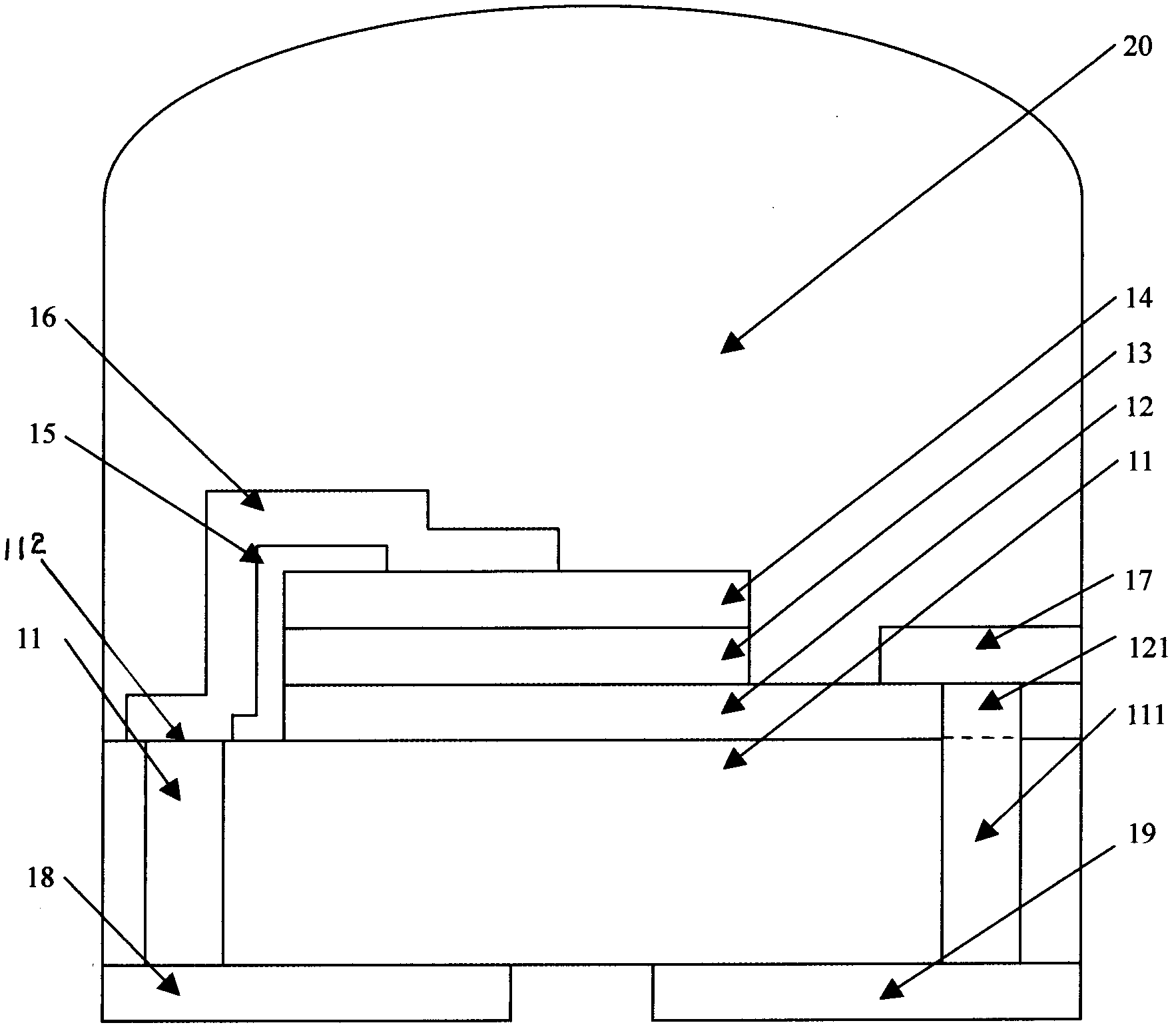
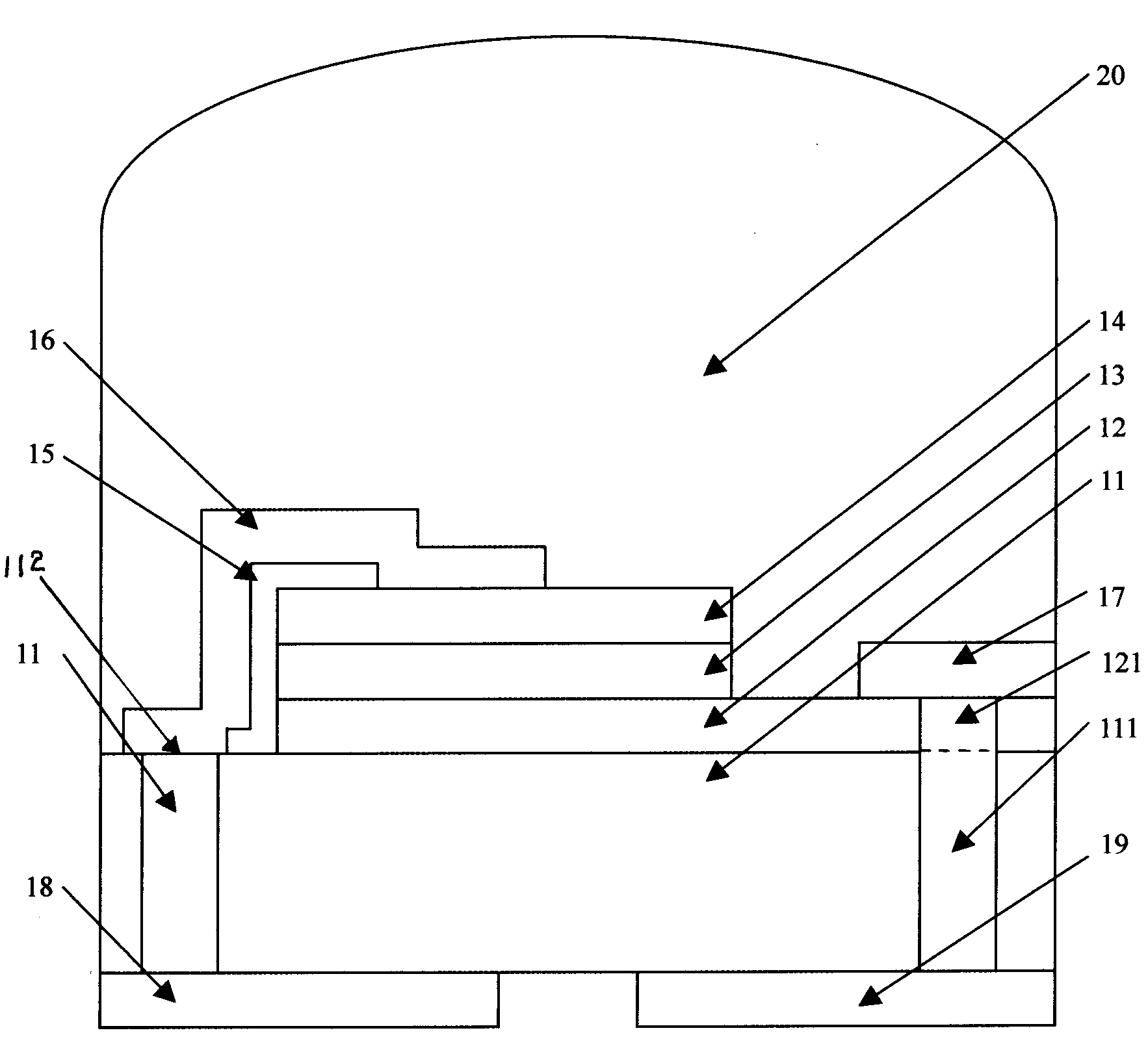
[0025] see figure 1 As shown, the present invention provides a light emitting diode packaging structure, including:

[0026] An insulating substrate 11, the two sides above the insulating substrate 11 have through holes 111, the through holes 111 are filled with conductive metal, the material of the insulating substrate 11 is sapphire or silicon carbide or aluminum nitride, its Good insulation performance; the thickness of the insulating substrate 11 can be thinner than the conventional process, less than 100um, which can effectively reduce the thermal resistance of the device; the through hole 111 is a round hole or a groove; the conductive metal filled in the through hole 111 For full filling or partial filling, the partial filling refers to filling a layer of conductive metal on the sidewall of the through hole 111;

[0027] An n-type layer 12, the n-type layer 12 is made on the insulating substrate 11, and covers most of the area of ​​the insulating substrate 11, so that ...


PUM


Abstract

The invention relates to a light emitting diode (LED) packaging structure. The LED packaging structure comprises an insulating substrate, an n-shaped layer, an active layer, a p-shaped layer; an isolating layer, a p electrode, an n electrode, a first back electrode and a second back electrode, wherein through holes are formed on both sides of the insulating substrate and are filled with conductive metal; the n-shaped layer is arranged on the insulating substrate, and a hole is formed in the n-shaped layer and is filled with conductive metal; the active layer is arranged on the n-shaped layer;the p-shaped layer is arranged on the active layer; the isolating layer is positioned on one side of the n-shaped layer, the active layer and the p-shaped layer and is used for covering a part of upper surface of the p-shaped layer; the p electrode is used for covering the isolating layer and covering a part of upper surface of the p-shaped layer; the n electrode is arranged on one side of the upper side of the n-shaped layer and is connected with the conductive metal in the through holes in the insulating substrate; the first back electrode is arranged on one side of the rear side of the insulating substrate and is connected with the p electrode through the conductive metal in the through holes in the insulating substrate; and the second back electrode is arranged on the other side of the rear side of the insulating substrate and is connected with the n electrode through the conductive metal in the through holes in the insulating substrate. A substrate of a device is formed by all the parts, and an optical element is packaged on the substrate to complete the production of the device.

Description

technical field [0001] The invention belongs to the technical field of semiconductors, in particular to a light-emitting diode packaging structure prepared by wafer-level in-situ packaging technology. Background technique [0002] At present, the preparation process of light-emitting diodes is generally divided into three main steps: material epitaxy, chip technology, and chip packaging. The basic function of semiconductor device packaging is to connect micro-sized chip electrodes to relatively large-sized electrode structures for practical use. [0003] The LED packaging process generally uses some kind of substrate, case or bracket, and the LED chip is bonded to the substrate, case or bracket in some way, and then the electrodes on the upper part of the chip are connected to each other through the gold wire ball bonding process. To the corresponding electrodes on the substrate, case or bracket to achieve electrical connection, and finally use a transparent packaging mater...

Claims


Application Information

Patent Timeline
IPC IPC(8): H01L33/48H01L33/62
Inventor 杨华卢鹏志谢海忠于飞郑怀文薛斌伊晓燕王军喜王国宏李晋闽
Owner INST OF SEMICONDUCTORS - CHINESE ACAD OF SCI
Why Eureka
Try Eureka