
Crystal grain structure of light-emitting diode and method for manufacturing bottom electrode of crystal grain structure

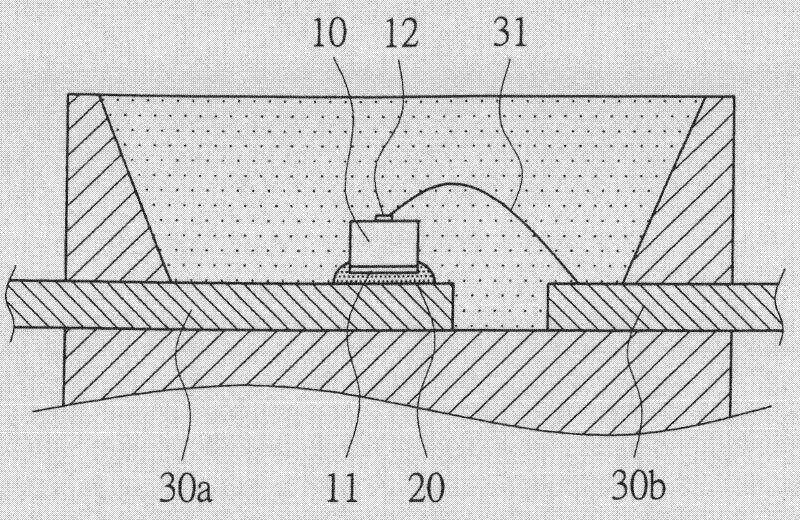
A technology of light-emitting diodes and grain structures, which is applied in the direction of circuits, electrical components, semiconductor devices, etc., and can solve the problem of deterioration in the electrical connection quality between the die-bonding glue 20 and the LED grain 10, electrical instability and gaps in LEDAssembly components, etc. problem, to achieve the effect of improving the quality of electrical connection

Inactive Publication Date: 2011-10-12
ARIMA OPTOELECTRONICS
View PDF4 Cites 2 Cited by
  • Summary
  • Abstract
  • Description
  • Claims
  • Application Information

AI Technical Summary

Problems solved by technology

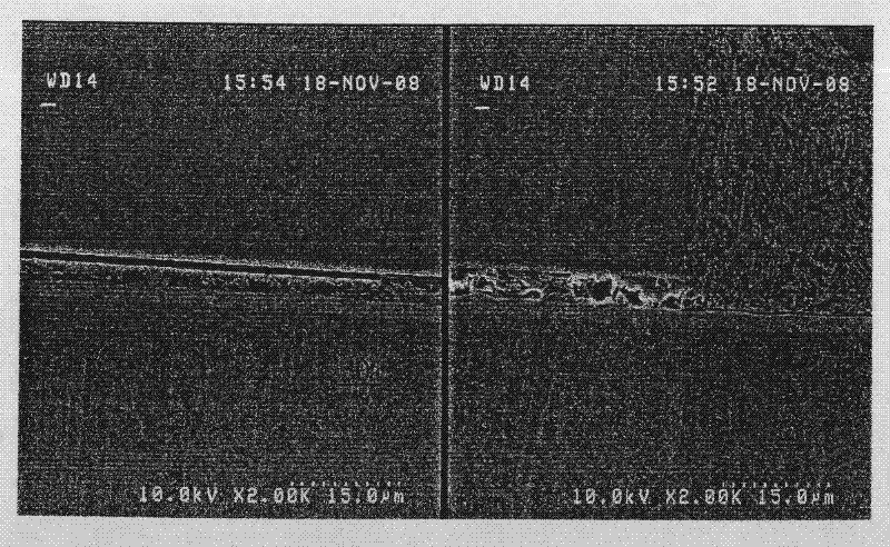
[0005] However, if figure 2 As shown in the cross-sectional photo of the die-bonding structure, it can be clearly seen that there are many bad joints (gap) on the joint surface between the bottom of the LED die 10 and the die-bonding adhesive 20, but the side of the LED die 10 is not connected to the die-bonding adhesive 20. 20 stays in good engagement
The above situation will cause the electrical instability of the LED Assembly component, especially when the cooling and heating cycle is applied, the quality of the electrical connection between the die-bonding adhesive 20 and the LED die 10 will be further deteriorated due to the expansion and contraction of the air in the gap.

Method used


Image

  • Crystal grain structure of light-emitting diode and method for manufacturing bottom electrode of crystal grain structure
  • Crystal grain structure of light-emitting diode and method for manufacturing bottom electrode of crystal grain structure
  • Crystal grain structure of light-emitting diode and method for manufacturing bottom electrode of crystal grain structure

Examples


Embodiment Construction

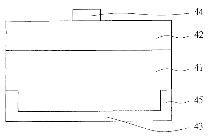
[0028] First, see image 3 , Figure 4 As shown, the light-emitting diode grain structure of the present invention includes:

[0029] a substrate 41;

[0030] a light-emitting layer 42 formed on the top surface of the substrate 41;

[0031] At least one bottom electrode 43 is formed on the bottom surface of the substrate 41;

[0032] At least one top surface electrode 44 is formed on the top surface of the light emitting layer 42;

[0033] At least one side electrode 45 is formed on the bottom side of the substrate 41 .

[0034] Based on the above structure, the light-emitting diode grain structure of the present invention improves the design of the electrodes. In addition to the bottom electrode 43 and the top electrode 44, a side electrode 45 of a certain height is provided at the bottom of the substrate 41; and when the package is completed Finally, the wire 31 is electrically connected to the top electrode 44 and the second lead frame 30b, and the die-bonding glue 20 ...


PUM


Abstract

The invention discloses a crystal grain structure of light-emitting diode and a method for manufacturing a bottom electrode of the crystal grain structure. The crystal grain structure of the light-emitting diode comprises a substrate, a light-emitting layer, at least one bottom surface electrode, at least one top surface electrode and at least one side surface electrode, wherein the light-emitting layer is formed on the top surface of the substrate; the bottom surface electrode is formed on the bottom surface of the substrate; the top surface electrode is formed on the top surface of the light-emitting layer; and the side surface electrode is formed on the bottom side surface of the substrate. In the method for manufacturing a bottom electrode, the crystal grain structure of the light-emitting diode comprises a substrate, a light-emitting layer, at least one bottom surface electrode, at least one top surface electrode and at least one side surface electrode, wherein the light-emitting layer is formed on the top surface of the substrate; the bottom surface electrode is formed on the bottom surface of the substrate; the top surface electrode is formed on the top surface of the light-emitting layer; and the side surface electrode is formed on the bottom side surface of the substrate. The method for manufacturing the bottom electrode comprises the following steps of: forming a groove with a certain depth on the bottom surface of a substrate of a light-emitting diode wafer; plating a metal film on a bottom surface and inside the groove with a metal plating technology; and cutting the wafer into crystal grains along the groove. The invention has the advantages of improving the electric connection quality between a die bonding adhesive and crystal grains of a light-emitting diode.

Description

technical field [0001] The present invention relates to a light-emitting diode grain structure and its bottom electrode manufacturing method, in particular to a bottom electrode including bottom surface and side electrodes, which can maintain stable electrical connection quality when applied to a vertical conduction type packaging structure. design. Background technique [0002] Light-emitting diode (LED) is a light source element with small size, high luminous efficacy and full color. Because of these characteristics, the application of light-emitting diodes is ever-changing, so many forms of assembly are derived; after packaging The products are commonly referred to as lamps (Lamp) or surface mount devices (SMD), and in addition to the main consideration of packaging for appearance, quality reliability is also an important consideration. Therefore, whether it is in the form of Lamp or SMD, the front stage of the packaging process includes an important step-Die bonding. P...

Claims


Application Information

Patent Timeline
Patent Type & Authority Applications(China)
IPC IPC(8): H01L33/36
Inventor 王会恒
Owner ARIMA OPTOELECTRONICS
Learn More