Semiconductor wafer electrode structure and manufacturing method thereof

A technology of wafer electrodes and manufacturing methods, applied in semiconductor/solid-state device manufacturing, semiconductor devices, semiconductor/solid-state device components, etc., can solve problems such as abnormality, asymmetric transmission, damage to the material of the light-emitting layer, electrical instability, etc. , to achieve the effect of improving the quality

Inactive Publication Date: 2011-10-12
ARIMA OPTOELECTRONICS
View PDF4 Cites 16 Cited by
  • Summary
  • Abstract
  • Description
  • Claims
  • Application Information

AI Technical Summary

Problems solved by technology

[0003] Next, the ball-shaped wire is usually achieved by using a wire bonder, and the core of the wire bonder is the bonding head (Bonding head) that applies pressure. The heat energy usually comes from the micro heater (Mini heater), but both pressure and heat come from the wire bonding head, which has a decisive impact on the wire bonding quality; but any mechanical equipment has its mechanical differences and instability (Fluctuation), for ball type wire bonding , because the most common problem caused by these differences is nothing more than wire offset, that is, the center position of the ball end deviates from the center of the electrode, which will cause the pressure and ultrasonic energy from the wire head to be abnormal and asymmetrical Transfer to the light-emitting layer area adjacent to the periphery of the electrode, and if some LED light-emitting layer materials are not hard enough (such as A1InGap) or have undergone special treatment (such as roughening), the above-mentioned energy will directly cause damage to the light-emitting layer material. Such as cracking (Crack, Cratering) damage, etc., which in turn cause the problem of yield loss and electrical instability of LED packaging components

Method used


Image

  • Semiconductor wafer electrode structure and manufacturing method thereof
  • Semiconductor wafer electrode structure and manufacturing method thereof
  • Semiconductor wafer electrode structure and manufacturing method thereof

Examples


Embodiment Construction

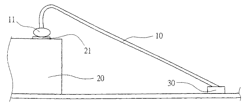
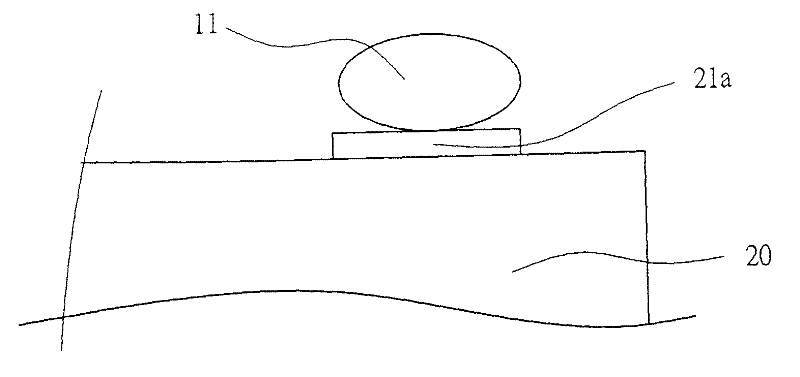
[0022] First, see figure 2 As shown, the surface of the electrode 21a of the existing semiconductor wafer 20 is a planar design; see also image 3 As shown, on the semiconductor wafer 20 of the same surface layer (such as the light-emitting layer of a light-emitting diode), an electrode 21b with a rough surface is made, and observing the wire-bonding process of the two forming the ball end 11, it can be known that the electrode 21b with a rough surface is larger than the electrode with a flat surface. 21a is more resistant to (offset) ultrasonic vibrations, which can be explained as the horizontal transmission of energy is hindered by the rough surface, and the vibration energy of ultrasonic waves is difficult to transmit downwards from both sides of the rough surface electrode 21b, so the bonding process causes the wafer to produce The possibility of chipping damage is less likely to occur under the rough surface electrode 21b, but the opposite is true for the flat surface e...


PUM


Abstract

The invention discloses a semiconductor wafer electrode structure and a manufacturing method thereof. According to the semiconductor wafer electrode structure, the centre area of the surface of an electrode is even and the periphery area of the surface of the electrode is rough; the attaching viscosity needed by wire bonding and ball junction ends is provided by the centre area; and the periphery area is used for preventing oscillation energy during wire bonding from being transversely transferred to the outer side of an electrode such that the ball junction ends joined with the electrode can accord with the wire bonding technical standard. The manufacturing method comprises the steps of: defining the centre area of the electrode on the surface layer of the semiconductor wafer by the mask lithography; roughening the area of the surface layer of the semiconductor chip beyond a photomask; and evaporating the electrode metal onto the flat and rough surfaces of the surface layer of the semiconductor wafer, and therefore the electrode structure with even surface centre area and rough periphery area is formed on the surface layer of the semiconductor wafer. The semiconductor wafer electric structure disclosed by the invention has the effect of enhancing the spherical wire bonding quality.

Description

technical field [0001] The invention relates to a semiconductor wafer electrode structure and manufacturing method, in particular to a design for making the central area of ​​the electrode surface flat and the peripheral area rough. Background technique [0002] Light-emitting diode (LED) is a light source element with small size, high luminous efficiency, and spans full colors. Therefore, its application methods are ever-changing, so many forms of assembly are derived. The packaged products are generally called Light (Lamp) or surface mount device (SMD), and the main consideration of packaging is not only appearance, but also quality reliability; therefore, whether it is Lamp form or SMD form, wire bonding (Wire bonding) is the packaging process An important step in the previous paragraph refers to the metal electrode (Pad) prepared on the front of the LED chip, using heat, pressure, and ultrasonic energy to adhere the metal to the electrode surface to form electrical condu...

Claims


Application Information

Patent Timeline
Patent Type & Authority Applications(China)
IPC IPC(8): H01L23/482H01L21/60H01L33/62
CPCH01L24/05H01L2224/04042H01L2224/05599H01L2224/451H01L2224/48H01L2224/48091H01L2224/48465H01L2224/85399H01L2924/00014H01L2924/12041H01L2224/45099H01L2924/00H01L2924/00012
Inventor 王会恒
Owner ARIMA OPTOELECTRONICS
Why Eureka
Try Eureka