Method for processing microstructure of silicon and metal composite material

A technology of metal composite materials and processing methods, which is applied in the field of microstructure production of silicon and metal composite materials, can solve the problems of inability to provide plastic deformation ability and limited improvement, and achieve perfect electroformed metal structure, good repeatability, and easy The effect of separation

Inactive Publication Date: 2011-08-31
TIANJIN SEAGULL WATCH CO LTD +1
View PDF10 Cites 4 Cited by
  • Summary
  • Abstract
  • Description
  • Claims
  • Application Information

AI Technical Summary

Problems solved by technology

This method can solve the assembly problem of metal parts and silicon parts to a certain extent, and reduce the scrap rate caused by assembly, but the improvement is limited, and the silicon elastic structure still cannot provide the effective plastic deformation capacity of the material required for assembly.

Method used


Image

  • Method for processing microstructure of silicon and metal composite material
  • Method for processing microstructure of silicon and metal composite material
  • Method for processing microstructure of silicon and metal composite material

Examples


Embodiment

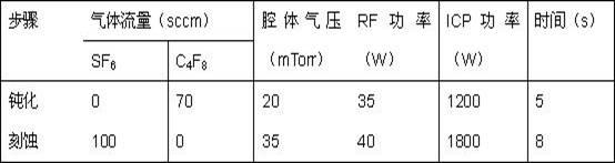
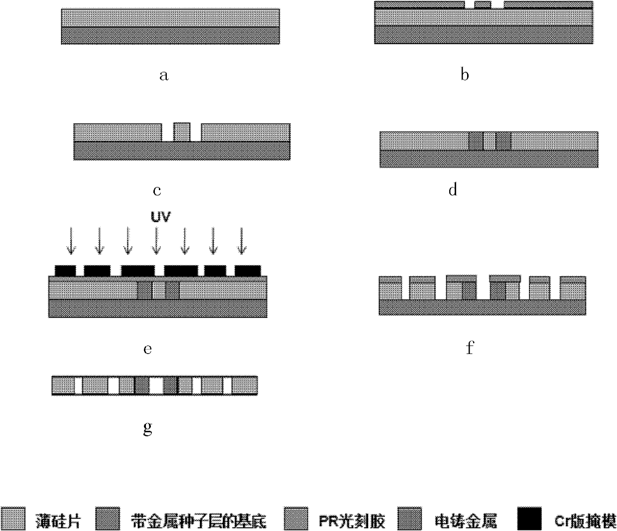
[0026] (1) Thin silicon wafer is eutectically bonded to a silicon substrate containing a metal seed layer, see figure 1 (a);

[0027] a) Select a thin silicon wafer with a size of 3", a thickness of 100um, and a crystal orientation of ;

[0028] b) Routine cleaning of the surface of the thin silicon wafer: add deionized water for ultrasonic cleaning for 10 minutes, then rinse with deionized water; add acetone and absolute ethanol for ultrasonic cleaning and then clean with deionized water; boil concentrated sulfuric acid and add hydrogen peroxide Wash with deionized water after rinsing with dilute hydrofluoric acid; rinse with deionized water after rinsing with dilute hydrofluoric acid; 2 Dry with infrared light under atmosphere;

[0029] c) Sputtering a Ti / Au / Ti metal seed layer on a silicon substrate (thickness 500um, crystal orientation ) with a thickness of 20 / 200 / 20 nm;

[0030] d) Realize the eutectic bonding of Si / Au in a vacuum nitrogen oven: temperature 420-450 d...


PUM


Abstract

The invention discloses a method for processing a microstructure of a silicon and metal composite material. The method comprises the following steps of: 1, performing congruent melting and bonding on a silicon wafer and a metal electroforming seed layer on a silicon substrate; 2, performing photoetching on an AZ short pimp electroforming metal pattern; 3, performing deep etching on a first layer of silicon structure; 4, filling a structure in electroforming metal; 5, performing photoetching on an AZ short pimp silicon structure pattern; 6, performing deep etching on a second layer of silicon structure; and 7, removing photoresist and separating the substrate to release the micro structure of the silicon and metal composite material. The method has the advantages that: the functional silicon wafer is bonded on the silicon substrate with the metal seed layer, etching is performed by using a reaction ion coupled dry method deep etching technology, a metal structure is electroformed, and other silicon structures are etched; the micro structure obtained by the method has high size accuracy, and the electroforming metal has a perfect structure; the silicon side wall which is subjected to deep etching has scallop-type strips, so that the electroformed metal structure and the silicon structure are meshed with each other and are not easy to separate and drop; moreover, the deep etching and electroforming process is adopted, so the repeatability is high.

Description

technical field [0001] The invention relates to the field of microprocessing; in particular, it relates to a microstructure manufacturing method of silicon and metal composite materials. Background technique [0002] In the final analysis, micro-nano processing is to fabricate micro-nano structures on various functional materials. The so-called functional materials are materials that can make various micro-nano devices, such as silicon and silicon dioxide, which are the most widely used materials in micro-mechanical and micro-fluidic systems, and are also the basic materials of the semiconductor industry. In 1960, R. Feymann defined the concept of micromachines in a lecture at Caltech. In 1962, the first silicon pressure sensor came out, and then developed microstructures such as 50-500 um gears, gear pumps, pneumatic turbines and connectors. In 1982, K.E. Peterson published a review article entitled "Silicon as a Mechanical Material", which laid the foundation for the dev...

Claims


Application Information

Patent Timeline
Patent Type & Authority Applications(China)
IPC IPC(8): B81C1/00
Inventor 郭育华王英男江争马广礼
Owner TIANJIN SEAGULL WATCH CO LTD
Why Eureka
Try Eureka