Manufacturing method of AlGaInP light-emitting diode
A technology of light-emitting diodes and manufacturing methods, which is applied to electrical components, circuits, semiconductor devices, etc., can solve the problems of not being suitable for small-sized light-emitting diodes, reducing the luminous efficiency of small-sized chips, reducing the light-emitting area of the front surface, etc., and achieving optimal current distribution. , improve light efficiency, avoid damage to the effect
- Summary
- Abstract
- Description
- Claims
- Application Information
AI Technical Summary
Problems solved by technology
Method used
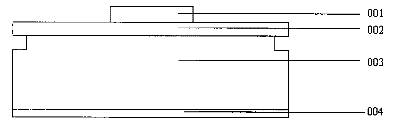
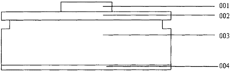
Image

Examples
Embodiment 1
[0022] Step 1: half-cut the AlGaInP light-emitting diode chip by contact scribing process, and the half-cut depth is 40-60um;
[0023] Step 2: Apply photoresist evenly on the back of the chip, and bake on a hot plate until the glue is dry;
[0024] Step 3: configure ammonia water corrosion solution, the ammonia water corrosion solution adopts ammonia water: hydrogen peroxide: water volume ratio is 1: 2: 1;
[0025] Step 4: Corrode the chip in the ammonia solution for 60 seconds with a flower basket;
[0026] Step 5: Rinse the chip with deionized water after corrosion;
[0027] Step 6: remove the photoresist on the back of the chip;
[0028] Step 7: Dry the chip with dry nitrogen.
[0029] sample
Brightnessmcd(20mA)
uncorroded
153.8
corrosion
158.6
[0030] Table 1: Comparison of optoelectronic performance parameters of chips
[0031] Referring to the experimental data in Table 1, the light intensity of the chip is 3.1% higher th...
Embodiment 2
[0033] Step 1: half-cut the AlGaInP light-emitting diode chip by contact scribing process, and the half-cut depth is 40-60um;
[0034] Step 2: Apply photoresist evenly on the back of the chip, and bake on a hot plate until the glue is dry;
[0035] Step 3: configure ammonia water corrosion solution, the ammonia water corrosion solution adopts ammonia water: hydrogen peroxide: water volume ratio is 1: 2: 1;
[0036] Step 4: Corrode the chip in the ammonia solution for 90 seconds with a flower basket;
[0037] Step 5: Rinse the chip with deionized water after corrosion;
[0038] Step 6: remove the photoresist on the back of the chip;
[0039] Step 7: Dry the chip with dry nitrogen.
[0040] sample
Brightnessmcd(20mA)
uncorroded
152
corrosion
165.4
[0041] Table 2: Comparison of optoelectronic performance parameters of chips
[0042] Referring to the experimental data in Table 2, the light intensity of the chip is 8.8% higher than...
Embodiment 3
[0044] Step 1: half-cut the AlGaInP light-emitting diode chip by contact scribing process, and the half-cut depth is 40-60um;
[0045] Step 2: Apply photoresist evenly on the back of the chip, and bake on a hot plate until the glue is dry;
[0046] Step 3: configure ammonia water corrosion solution, the ammonia water corrosion solution adopts ammonia water: hydrogen peroxide: water volume ratio is 1: 2: 1;
[0047] Step 4: Corrode the chip in the ammonia solution for 120 seconds with a flower basket;
[0048] Step 5: Rinse the chip with deionized water after corrosion;
[0049] Step 6: remove the photoresist on the back of the chip;
[0050] Step 7: Dry the chip with dry nitrogen.
[0051] sample
Brightnessmcd(20mA)
uncorroded
152.7
corrosion
175
[0052] Table 3: Comparison of optoelectronic performance parameters of chips
[0053] Referring to the experimental data in Table 3, the light intensity of the chip is 14.6% higher th...
PUM
 Abstract
Description
Claims
Application Information
 - R&D
- Intellectual Property
- Life Sciences
- Materials
- Tech Scout
- Unparalleled Data Quality
- Higher Quality Content
- 60% Fewer Hallucinations
Browse by: Latest US Patents, China's latest patents, Technical Efficacy Thesaurus, Application Domain, Technology Topic, Popular Technical Reports.
© 2025 PatSnap. All rights reserved.Legal|Privacy policy|Modern Slavery Act Transparency Statement|Sitemap|About US| Contact US: help@patsnap.com