Method for preparing moth-eye structure for antireflection on surface of solar battery
A technology of solar cells and solar cells, which is applied in the manufacture of circuits, electrical components, and final products. It can solve the problems of poor long-range periodicity and the lack of versatility of semiconductor substrates, and achieves the suppression of interface reflection, low cost, and good anti-reflection effect of effect
- Summary
- Abstract
- Description
- Claims
- Application Information
AI Technical Summary
Problems solved by technology
Method used
Image
Examples
preparation example Construction
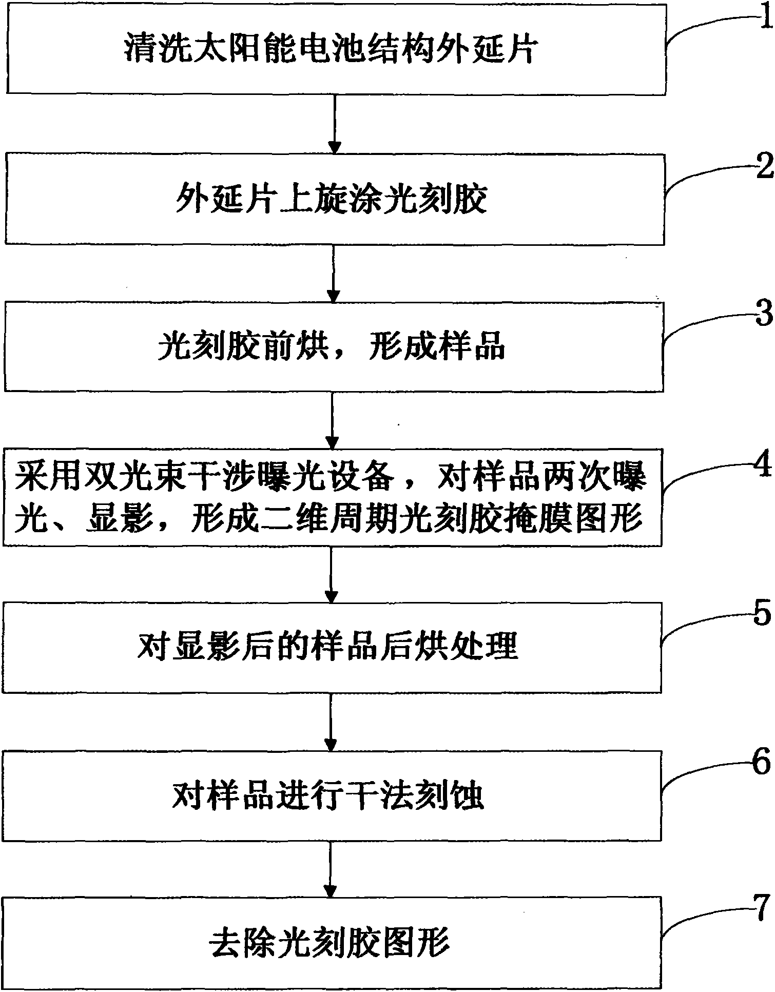
[0024] see figure 1 , Shown in 2, 3, a kind of preparation method of the moth-eye structure that is used for solar cell surface anti-reflection of the present invention, comprises the following steps:
[0025] Step 1: Take an epitaxial wafer used for a solar cell, and clean the epitaxial wafer, the epitaxial wafer is a monocrystalline Si or GaAs-based solar cell structure;
[0026] The cleaning method of GaAs-based epitaxial wafers is as follows: place the epitaxial wafers in acetone and absolute ethanol respectively, heat them at 55°C for 3-5 minutes, then rinse them with deionized water, dry them with nitrogen, and then put them in the negative film remover Boil in medium for 15 minutes, rinse with deionized water, and then bake in an oven at 120°C for 30 minutes; for Si-based epitaxial wafers, use standard RCA cleaning method to improve the adhesion of photoresist to the substrate.
[0027] Step 2: Spin-coat the photoresist on the epitaxial wafer, and the photoresist used ...
example 1
[0056] Example 1: Rhomboid GaAs moth-eye surface anti-reflection structure
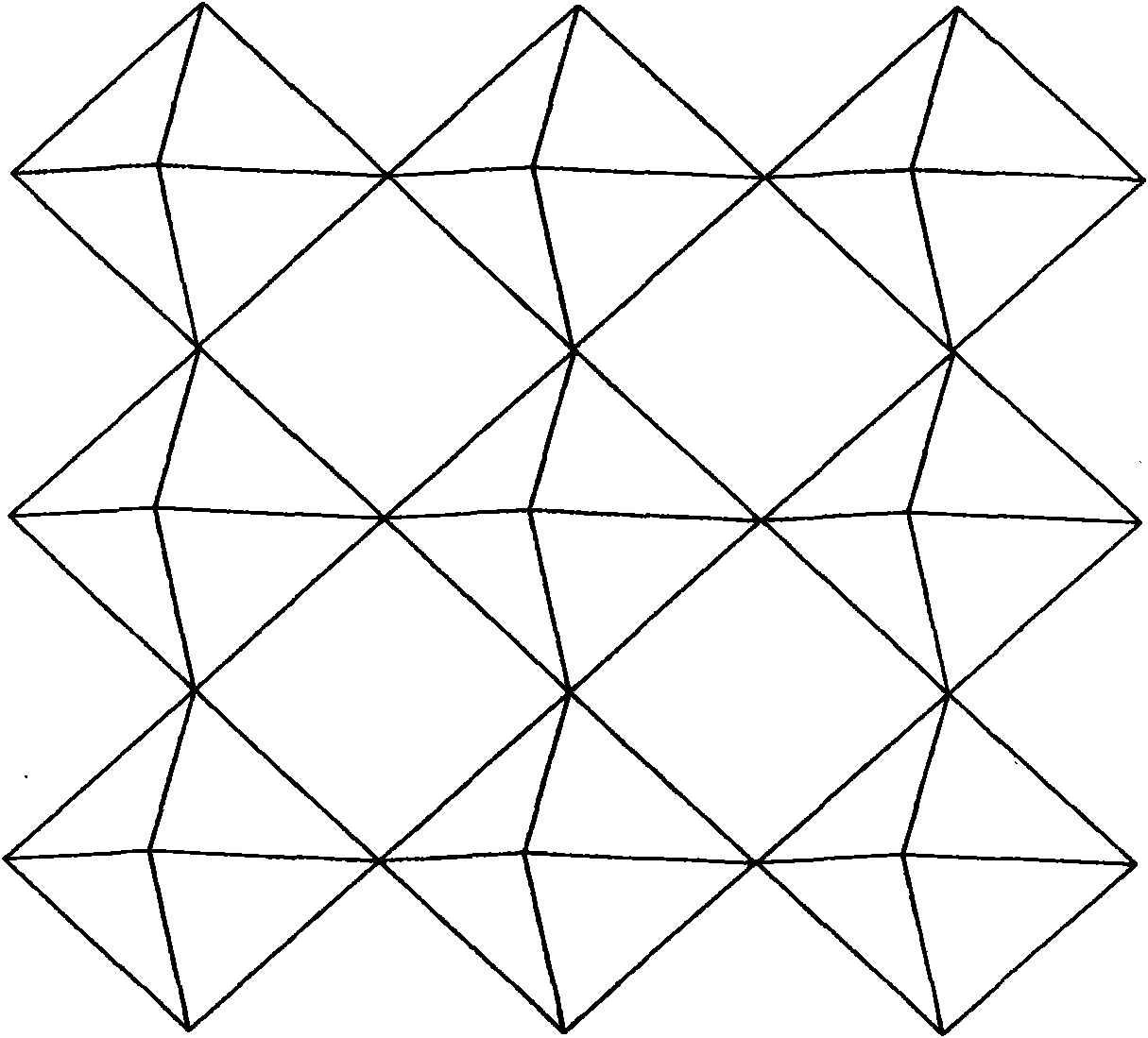
[0057] To prepare anti-reflection structures on the diamond-shaped GaAs moth-eye surface, a pseudo-diamond array photoresist mask is needed. see image 3 The two-dimensional distribution of the exposure dose shown should ideally be diamond-shaped rather than a hole array. However, due to the isotropy of the development process and the spatial fluctuation of the exposure dose during the exposure process, the actual shape obtained is not ideal. Rhombus shape. However, the duty ratio of the pseudo-rhomboid is 1, which is greater than that of the circular array photoresist mask prepared by the usual method with a duty ratio of only 0.5. After dry etching, a diamond-shaped moth-eye structure similar to that shown in Figure 2(a) is obtained, with a duty cycle of 1 and a depth of 450nm. The reflectance spectrum measured under the condition of incident angle of 8 degrees of arbitrary polarized light is as ...
example 2
[0058] Example 2: Conical GaAs moth-eye surface anti-reflection structure
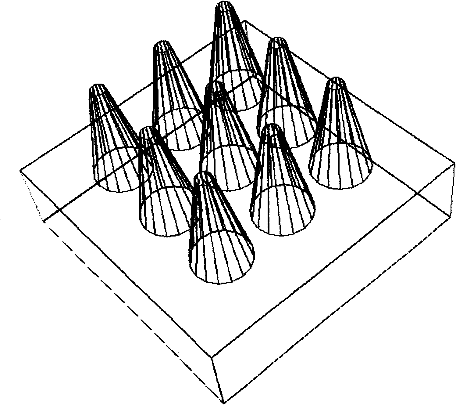
[0059] The conical GaAs moth-eye structure was prepared, and the conical structure as shown in Figure 2(b) was obtained by dry etching using a two-dimensional periodic circular lattice mask. The specific steps are: (1) spin-coat 120nm-thick photoresist on the GaAs substrate; (2) bake in an oven at 90°C for 20 minutes; (3) expose with a double-beam interference exposure system, and rotate the substrate between two exposures 90 degrees, to get a square lattice; (4) control the exposure, so that image 3 The area larger than the contour line 2 shown is fully exposed, resulting in a potential circular hole array; (5) careful control of the development time, revealing a two-dimensional circular dot matrix array; (6) post-baking; (7) ICP dry method etch. The prepared conical GaAs moth-eye structure is similar to that in Figure 2(b), with a depth of about 400nm and a duty ratio between 0.5-0.6. In the case...
PUM
| Property | Measurement | Unit |
|---|---|---|
| thickness | aaaaa | aaaaa |
| thickness | aaaaa | aaaaa |
| thickness | aaaaa | aaaaa |
Abstract
Description
Claims
Application Information
 - R&D
- Intellectual Property
- Life Sciences
- Materials
- Tech Scout
- Unparalleled Data Quality
- Higher Quality Content
- 60% Fewer Hallucinations
Browse by: Latest US Patents, China's latest patents, Technical Efficacy Thesaurus, Application Domain, Technology Topic, Popular Technical Reports.
© 2025 PatSnap. All rights reserved.Legal|Privacy policy|Modern Slavery Act Transparency Statement|Sitemap|About US| Contact US: help@patsnap.com


