Magnetic multilayer film unit, preparation method and magnetic moment overturning method thereof
A multi-layer film and magnetic technology, applied in the field of spintronics, can solve the problems of difficult mass production, mismatch of semiconductor CMOS circuits, and the inability to reduce the critical switching current density, so as to broaden the application range, reduce power consumption, The effect of increasing the degree of integration
- Summary
- Abstract
- Description
- Claims
- Application Information
AI Technical Summary
Problems solved by technology
Method used
Image


Examples
Embodiment 1
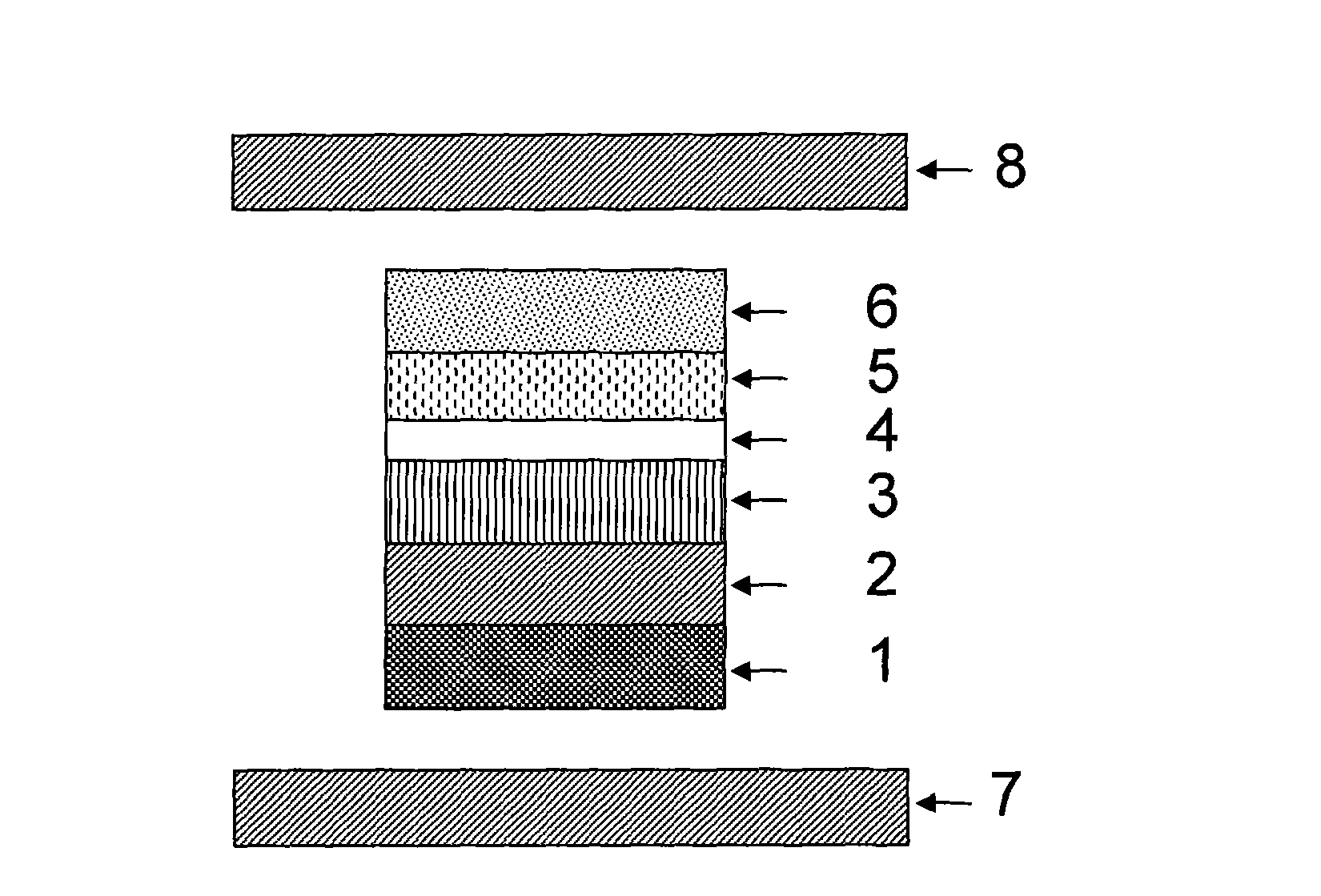
[0051] This embodiment provides a magnetic multi-layer film unit based on a vertical film surface electric field. Such as figure 1 As shown, the magnetic multilayer film unit of this embodiment includes a magnetic multilayer film core unit and a magnetic moment control unit.
[0052] Among them, the multilayer film core unit adopts a single barrier structure, including buffer layer 1, pinning layer 2, pinned layer 3, barrier layer 4, free layer 5 and covering layer 6 from bottom to top. The magnetic moment control unit includes two conductive layers 7, 8, the two conductive layers 7, 8 are all parallel to the film surface of the magnetic multilayer film core unit, and the multilayer film core unit is located between the two conductive layers 7, 8, That is, the core unit of the multilayer film is located in the electric field formed by the two conductive layers 7 , 8 . In this embodiment, there is an insulating layer between the conductive layer of the multilayer film core un...
Embodiment 2
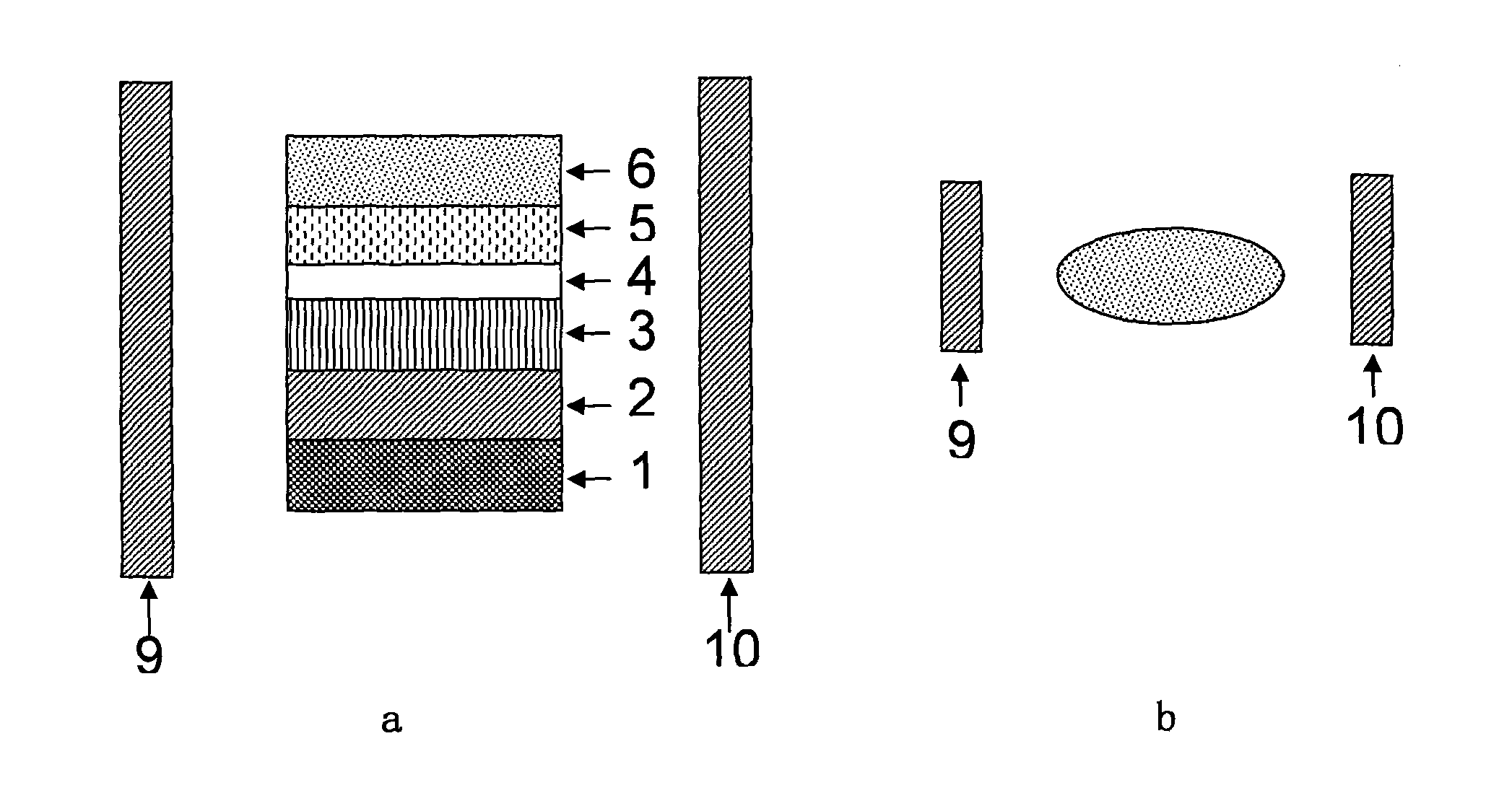
[0064] This embodiment provides a magnetic multilayer film unit based on the electric field parallel to the film surface. Such as figure 2 as shown,
[0065] The magnetic multilayer film unit of the present embodiment comprises a magnetic multilayer film core unit and a magnetic moment control unit,
[0066] Among them, the multilayer film core unit adopts a single barrier structure, including buffer layer 1, pinning layer 2, pinned layer 3, barrier layer 4, free layer 5 and covering layer 6 from bottom to top. The magnetic moment control unit includes two conductive layers 9, 10, the two conductive layers 9, 10 are perpendicular to the film surface of the magnetic multilayer film core unit, and the multilayer film core unit is located between the two conductive layers 9, 10, That is, the core unit of the multilayer film is located in the electric field formed by the two conductive layers 9 , 10 . In this embodiment, there is an insulating layer between the conductive laye...
Embodiment 3
[0071] This embodiment provides a magnetic multilayer film unit based on localized parallel film surface electric field.
[0072] according to image 3 As shown, the magnetic multilayer film unit includes a magnetic multilayer film core unit and a magnetic moment control unit. Among them, the multilayer film core unit adopts a single barrier structure, including buffer layer 1, pinning layer 2, pinned layer 3, barrier layer 4, free layer 5 and covering layer 6 from bottom to top. The magnetic moment control unit includes two conductive layers 11, 12, and the free layer of the multilayer film core unit is located between the two conductive layers 11, 12, that is, the free layer of the multilayer film core unit is located between the two conductive layers 11, 12. in the electric field formed. The direction of two conductive layers 11,12 is consistent with embodiment 2, the difference between the conductive layers 11,12 of the present embodiment and the conductive layer of embo...
PUM
| Property | Measurement | Unit |
|---|---|---|
| Thickness | aaaaa | aaaaa |
| Thickness | aaaaa | aaaaa |
| Thickness | aaaaa | aaaaa |
Abstract
Description
Claims
Application Information
 - R&D
- Intellectual Property
- Life Sciences
- Materials
- Tech Scout
- Unparalleled Data Quality
- Higher Quality Content
- 60% Fewer Hallucinations
Browse by: Latest US Patents, China's latest patents, Technical Efficacy Thesaurus, Application Domain, Technology Topic, Popular Technical Reports.
© 2025 PatSnap. All rights reserved.Legal|Privacy policy|Modern Slavery Act Transparency Statement|Sitemap|About US| Contact US: help@patsnap.com