
Method for manufacturing self-alignment metal interconnection wire

A technology of metal interconnection lines and manufacturing methods, which is applied in semiconductor/solid-state device manufacturing, electrical components, circuits, etc., can solve the problems of small minimum distances between metal interconnection lines and gate conductive layers and gate layers.

Inactive Publication Date: 2011-04-27
SEMICON MFG INT (SHANGHAI) CORP
View PDF5 Cites 7 Cited by
  • Summary
  • Abstract
  • Description
  • Claims
  • Application Information

AI Technical Summary

Problems solved by technology

[0007] Therefore, the present invention provides a method for manufacturing self-aligned metal interconnects to solve the gap between the metal interconnects and the gate conductive layer and gate layer formed in the existing self-aligned metal interconnects. The problem that the minimum distance is too small

Method used


Image

  • Method for manufacturing self-alignment metal interconnection wire
  • Method for manufacturing self-alignment metal interconnection wire
  • Method for manufacturing self-alignment metal interconnection wire

Examples


Embodiment Construction

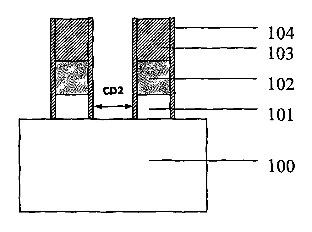
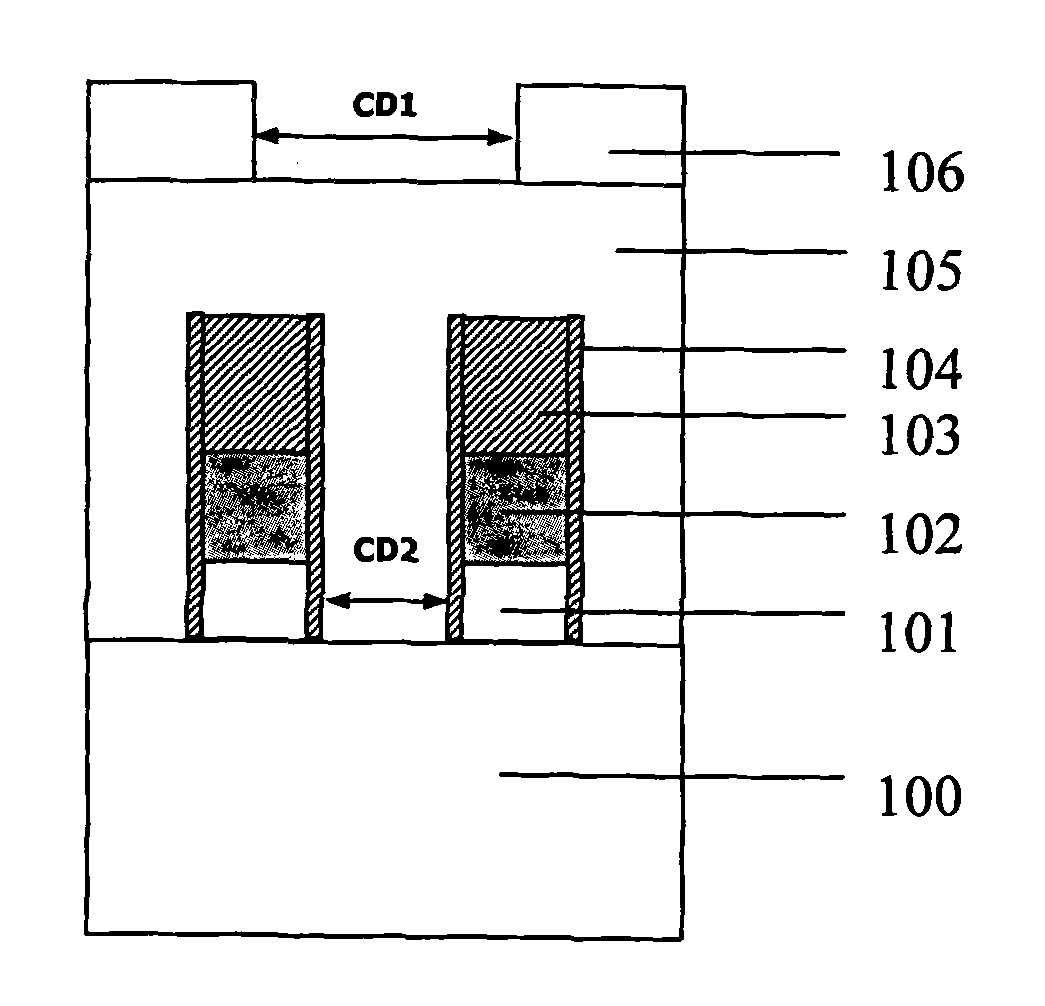
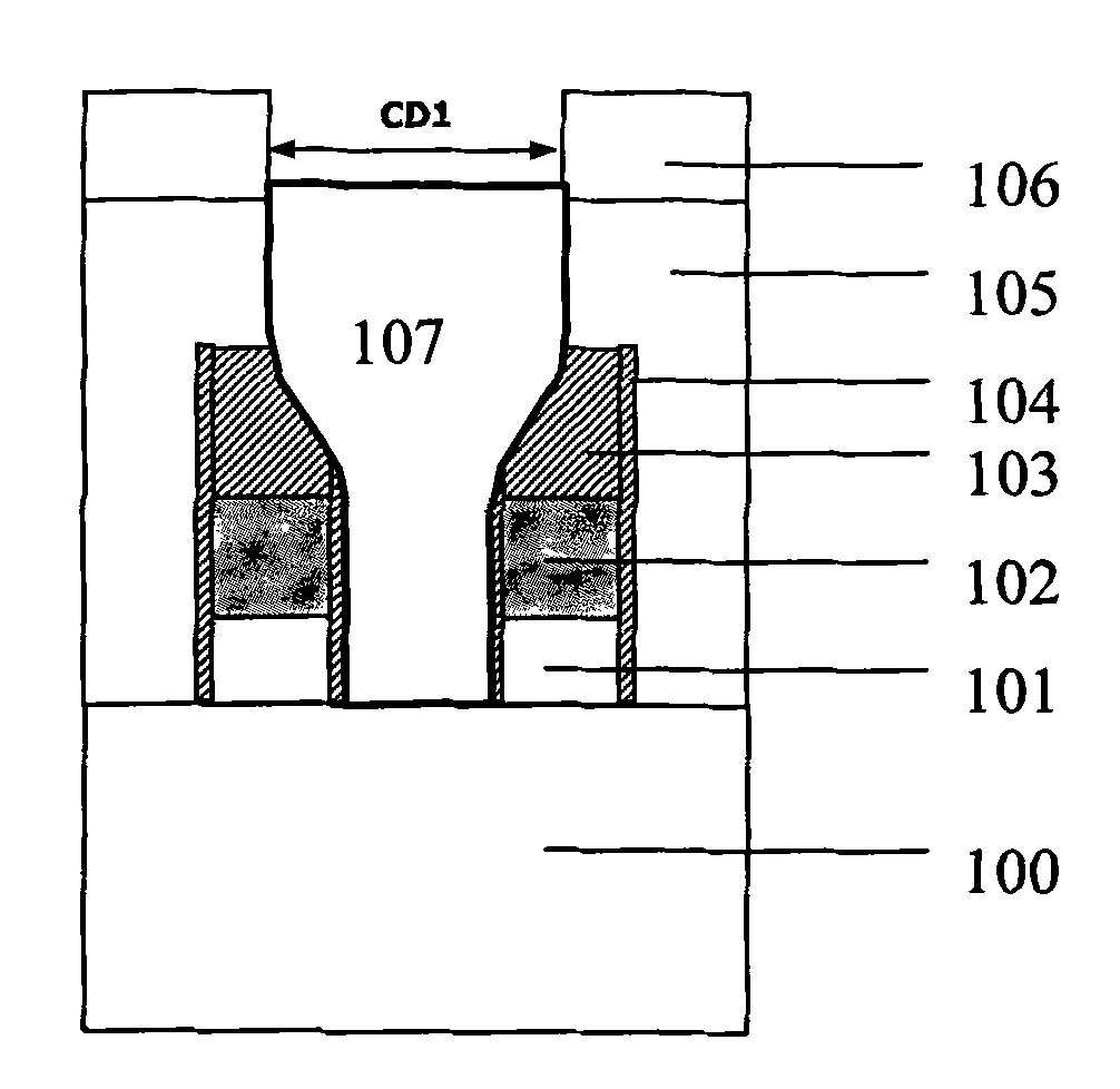
[0030] The method for manufacturing the self-aligned metal interconnection in this embodiment firstly provides a semiconductor substrate with more than one gate structure, and the gate structure consists of a gate layer, a gate conductive layer and a first hard mask sequentially located on the semiconductor substrate. Layer composition, and then form a first photoresist layer with a surface height higher than the gate structure on the semiconductor substrate and the gate structure; then plasma etch the first photoresist layer to expose the first mask layer and a part of the gate conductive layer; etching the exposed part of the gate conductive layer to cause a recess; removing the first photoresist layer; forming sidewalls on both sides of the gate structure; through the above process, the first mask layer and the gate conductive layer, the spacer will fill the recess produced by etching the gate conductive layer, therefore, the thickness of the sidewall at the interface positi...


PUM

PropertyMeasurementUnit
Thicknessaaaaaaaaaa
Thicknessaaaaaaaaaa
Thicknessaaaaaaaaaa

Abstract

The invention discloses a method for manufacturing a self-alignment metal interconnection wire, comprising the following steps of: providing a semiconductor substrate with more than one grid electrode structure, wherein the grid electrode structure comprises a grid electrode layer, a grid conducting layer and a first hard mask layer which are successively positioned on the semiconductor substrate; forming a first photoresist layer of which the surface is higher the grid electrode structure; etching the first photoresist layer with plasmas, and exposing the first mask layer and partial grid conducting layer; etching the exposed grid conducting layer to cause sinks generating on the grid conducting layer; removing the first photoresist layer; forming side walls, for filling the sinks, on two sides of the grid electrode structure; forming inter-layer dielectric layers on the semiconductor substrate and the grid electrode structure; etching the inter-layer dielectric layers to the semiconductor substrate and forming a contact hole on a set position; and filling a metal layer into the contact hole to form the metal interconnection wire. With the method, the thickness of an insulation layer between the grid conducting layer and the metal interconnection wire is increased, and the phenomenon of breakdown between the grid conducting layer and the metal interconnection wire can be avoided.

Description

technical field [0001] The invention relates to the technical field of semiconductor manufacturing, in particular to a method for manufacturing self-aligned metal interconnection lines. Background technique [0002] With the rapid development of ultra-large scale integration (ULSI, Ultra Large Scale Integration), the feature size (Feature Size) of components is getting smaller and the density is increasing, and the manufacturing process of integrated circuits is becoming more and more complex and sophisticated. The step process, especially the photolithography process, puts forward higher requirements. In this case, the self-alignment technology has attracted extensive attention because it can reduce the requirement for photolithographic precision, thereby reducing the area required for forming transistors. For example, in semiconductor process manufacturing, a self-aligned contact (SAC, self alignment contact) technology is often used to form self-aligned contact holes. F...

Claims


Application Information

Patent Timeline
IPC IPC(8): H01L21/768H01L21/8234H01L21/28
Inventor 邹立罗飞
Owner SEMICON MFG INT (SHANGHAI) CORP
Learn More