N-InP-based monolithic integrated optical logic gate and manufacturing method thereof

A monolithic integration, optical logic technology, applied in the direction of logic circuits using optoelectronic devices, logic circuits using specific components, logic circuits, etc.

Inactive Publication Date: 2011-04-20
INST OF SEMICONDUCTORS - CHINESE ACAD OF SCI
View PDF0 Cites 10 Cited by
  • Summary
  • Abstract
  • Description
  • Claims
  • Application Information

AI Technical Summary

Problems solved by technology

Single-line carrier photodetectors have attracted much attention due to their excellent speed and output performance. However, at present, the design and manufacture of similar devices in the world use detectors with surface-incidence structures, which will not solve the contradiction between efficiency and speed. Using semi-insulating Fe-InP doped as the substrate will increase the complexity of device fabrication

Method used


Image

  • N-InP-based monolithic integrated optical logic gate and manufacturing method thereof
  • N-InP-based monolithic integrated optical logic gate and manufacturing method thereof
  • N-InP-based monolithic integrated optical logic gate and manufacturing method thereof

Examples


Embodiment Construction

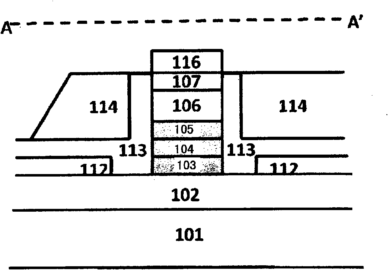
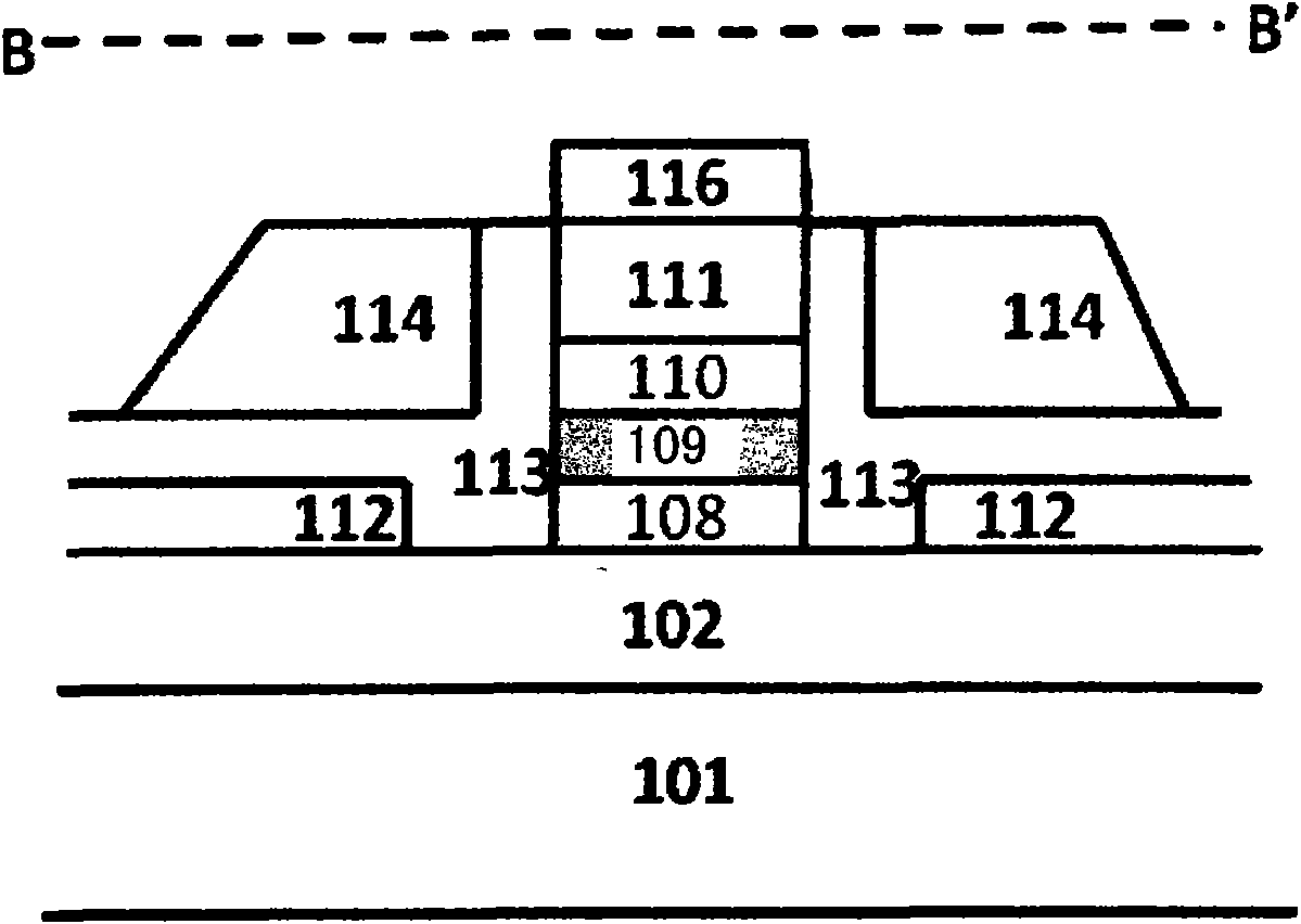
[0014] see Figure 1A -C, the present invention is based on n-InP monolithically integrated optical logic gate, comprising:

[0015] A substrate 101, which is an n-type (100) InP substrate, such as Figure 1A shown;

[0016] An n-type diluted waveguide layer 102. The n-type diluted waveguide layer 102 is fabricated on the substrate 101. The n-type diluted waveguide layer 102 is composed of 5-10 cycles of InP layers and InGaAsP layers alternately, and the doping concentration is 1×10 18 cm -3 ; wherein the bandgap wavelength of the InGaAsP layer is between 1.1-1.3 μm, which matches the lattice constant of the InP substrate; the total thickness of the diluted waveguide layer 102 is 1.5-4 μm, and the introduction of the diluted waveguide layer 102 can greatly improve the fiber- The coupling efficiency of the waveguide.

[0017] An undoped InGaAsP lower confinement layer 103, an undoped multi-quantum well layer 104, an undoped InGaAsP upper confinement layer 105, a p-type heavi...


PUM

PropertyMeasurementUnit
wavelengthaaaaaaaaaa
thicknessaaaaaaaaaa
wavelengthaaaaaaaaaa

Abstract

The invention discloses an n-InP-based monolithic integrated optical logic gate. The gate comprises a substrate, an n type diluting waveguide layer, a lower limit layer, a multiple quantum well layer, an upper limit layer, a cover layer, a contact layer, an N type wide bandgap layer, a P type narrow bandgap absorption layer, a P type heavily doped InP electronic barrier layer, a P type heavily doped InGaAs contact layer, an n type metal electrode layer, a silicon nitride or silicon oxide isolating coating, a polymer cladding, a film resistor, a P type microstrip linear metal electrode and a P type electrode board, wherein the n type diluting waveguide layer is manufactured on the substrate; the lower limit layer, the multiple quantum well layer, the upper limit layer, the cover layer and the contact layer are sequentially manufactured on the n type diluting waveguide layer to form an electric absorption modulator structure; the N type wide bandgap layer, the P type narrow bandgap absorption layer, the P type heavily doped InP electronic barrier layer and the P type heavily doped InGaAs contact layer are sequentially manufactured on the n type diluting waveguide layer to form single-row current carrier detector structure; the n type metal electrode layer is manufactured on the n type diluting waveguide layer; the silicon nitride or silicon oxide isolating coating is manufactured on the n type metal electrode layer and covers the side surfaces and surroundings of the electric absorption modulator structure and the single-row current carrier detector structure; the polymer cladding is manufactured on the silicon nitride or silicon oxide isolating coating; the film resistor is manufactured on the polymer cladding; and the P type microstrip linear metal electrode and the P type electrode board are manufactured on the polymer cladding and are connected through the film resistor.

Description

technical field [0001] The invention belongs to the field of optoelectronic integration (OEIC), in particular to a monolithic integrated waveguide type unidirectional carrier detector (WG-UTC-PD) and an inner step quantum well electroabsorption modulator (IQW) on an n-InP substrate. -EAM) and thin film resistors and MIM capacitors to realize the technical scheme and manufacturing method of optical logic AND gates. Background technique [0002] The current optical communication network is a photoelectric hybrid network, and the transmission capacity of information in optical fibers is extremely large, which has reached more than 20Tbit / s at present; however, the processing speed of information on optical network nodes can only reach the order of Gbit / s, and the information on network nodes Processing speed is currently the bottleneck of optical network performance improvement. Among the current methods of optical information processing, the traditional photoelectric-optical ...

Claims


Application Information

Patent Timeline
Patent Type & Authority Applications(China)
IPC IPC(8): G02F3/00
Inventor 张云霄廖栽宜周帆赵玲娟王圩
Owner INST OF SEMICONDUCTORS - CHINESE ACAD OF SCI
Why Eureka
Try Eureka