Groove MOSFET (Metal-Oxide Semiconductor Field Effect Transistor) device and making method thereof

A trench and trench gate technology is applied in the field of trench MOSFET devices and their manufacturing, which can solve problems such as over-etching, and achieve the effects of reducing Rds, reducing Qgd, and avoiding short-circuits.

Inactive Publication Date: 2011-04-13
FORCE MOS TECH CO LTD
View PDF0 Cites 13 Cited by
  • Summary
  • Abstract
  • Description
  • Claims
  • Application Information

AI Technical Summary

Problems solved by technology

Especially in the trench MOSFET whose trench gate depth is less than 1.0 μm, the above phenomenon can easily lead to the occurrence of over-etching, that is, the deeper gate contact trench will pass through the trench gate 110 ′ and extend into the epitaxial layer 102, thereby resulting in a gate-drain short circuit, as shown in Figure 1B

Method used


Image

  • Groove MOSFET (Metal-Oxide Semiconductor Field Effect Transistor) device and making method thereof
  • Groove MOSFET (Metal-Oxide Semiconductor Field Effect Transistor) device and making method thereof
  • Groove MOSFET (Metal-Oxide Semiconductor Field Effect Transistor) device and making method thereof

Examples


Embodiment Construction

[0055] The invention is explained in more detail below with reference to the accompanying drawings, in which preferred embodiments of the invention are shown. The invention can, however, be embodied in different ways and should not be limited to the embodiments described herein. For example, the description here refers more to N-channel trench MOSFETs, but clearly other devices are possible.

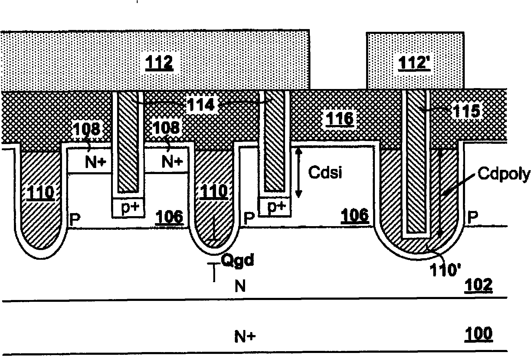
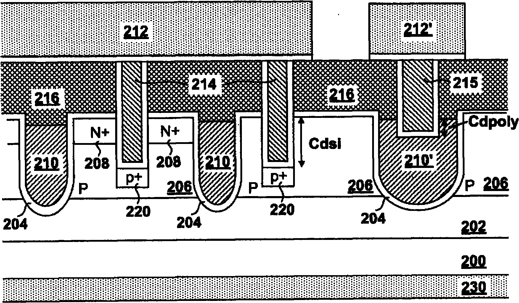
[0056] refer to figure 2 A preferred embodiment of the invention is shown. The N-channel trench MOSFET according to the preferred embodiment is formed on an N+ doped substrate 200, and a drain metal layer 230 is deposited on the lower surface of the substrate. The N-type epitaxial layer 202 is formed on the upper surface of the substrate 200 and has a lower majority carrier concentration than the substrate. In the epitaxial layer 200, a plurality of gate trenches 210 located in the active region and at least one wider gate trench 210' for gate contact are formed, and the trenches in t...


PUM


Abstract

The invention discloses a groove MOSFET (Metal-Oxide Semiconductor Field Effect Transistor) structure and a making method. In the structure, the depth of a gate contacting with a groove in a groove gate is smaller than that of a source body contacting with the groove in a body region. The groove MOSFET is adopted to efficiently prevent short circuit between the gate and drain caused by over etching of the gate contacting with the groove.

Description

technical field [0001] The invention mainly relates to a unit structure and a manufacturing method of a semiconductor power device. In particular, it relates to an improved trench MOSFET (Metal Oxide Semiconductor Field Effect Transistor) structure and its novel manufacturing method, so that the trench MOSFET structure can avoid gate-drain short circuit. Background technique [0002] An N-channel trench MOSFET device using a trench-type gate contact region and a trench-type source-body contact region in the prior art is shown in FIG. 1A . The structure of the N-channel trench MOSFET includes: a substrate 100 of N+ conductivity type; an epitaxial layer 102 of N conductivity type; a P-type body region 106; an N+ source region 108; a plurality of trench gates 110 located in the active region and At least one trench gate 110' for gate contact, the trench gates 110 and 110' are filled with polysilicon; source metal 112; gate metal 112'; trenched source-body contact region 114; t...

Claims


Application Information

Patent Timeline
Patent Type & Authority Applications(China)
IPC IPC(8): H01L29/78H01L29/38H01L29/06H01L29/423H01L29/49H01L29/417H01L23/52H01L21/336H01L21/311H01L21/28H01L21/265H01L21/266H01L21/324H01L21/768
CPCH01L2924/0002
Inventor 谢福渊
Owner FORCE MOS TECH CO LTD
Why Eureka
Try Eureka